
Method of programming a nonvolatile memory device using hybrid local boosting

a nonvolatile memory and local boost technology, applied in the field of nonvolatile memory device programming, can solve problems such as aggravated program disturban

Active Publication Date: 2008-01-31
SAMSUNG ELECTRONICS CO LTD
View PDF2 Cites 11 Cited by
  • Summary
  • Abstract
  • Description
  • Claims
  • Application Information

AI Technical Summary

Benefits of technology

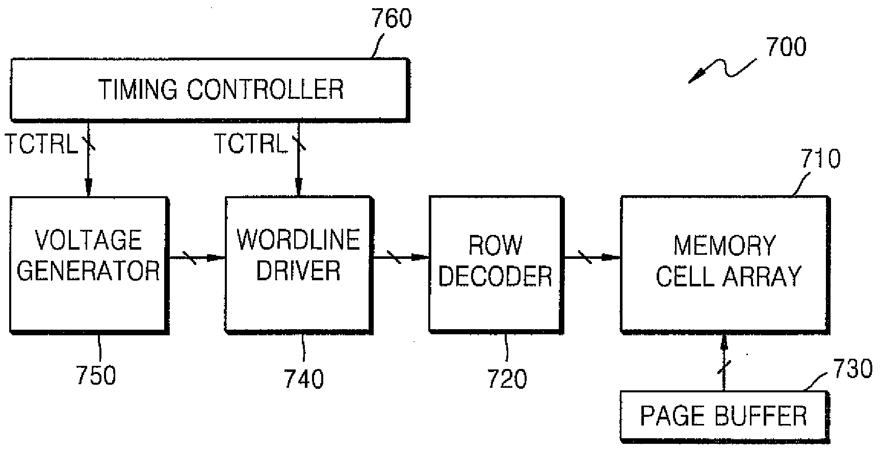
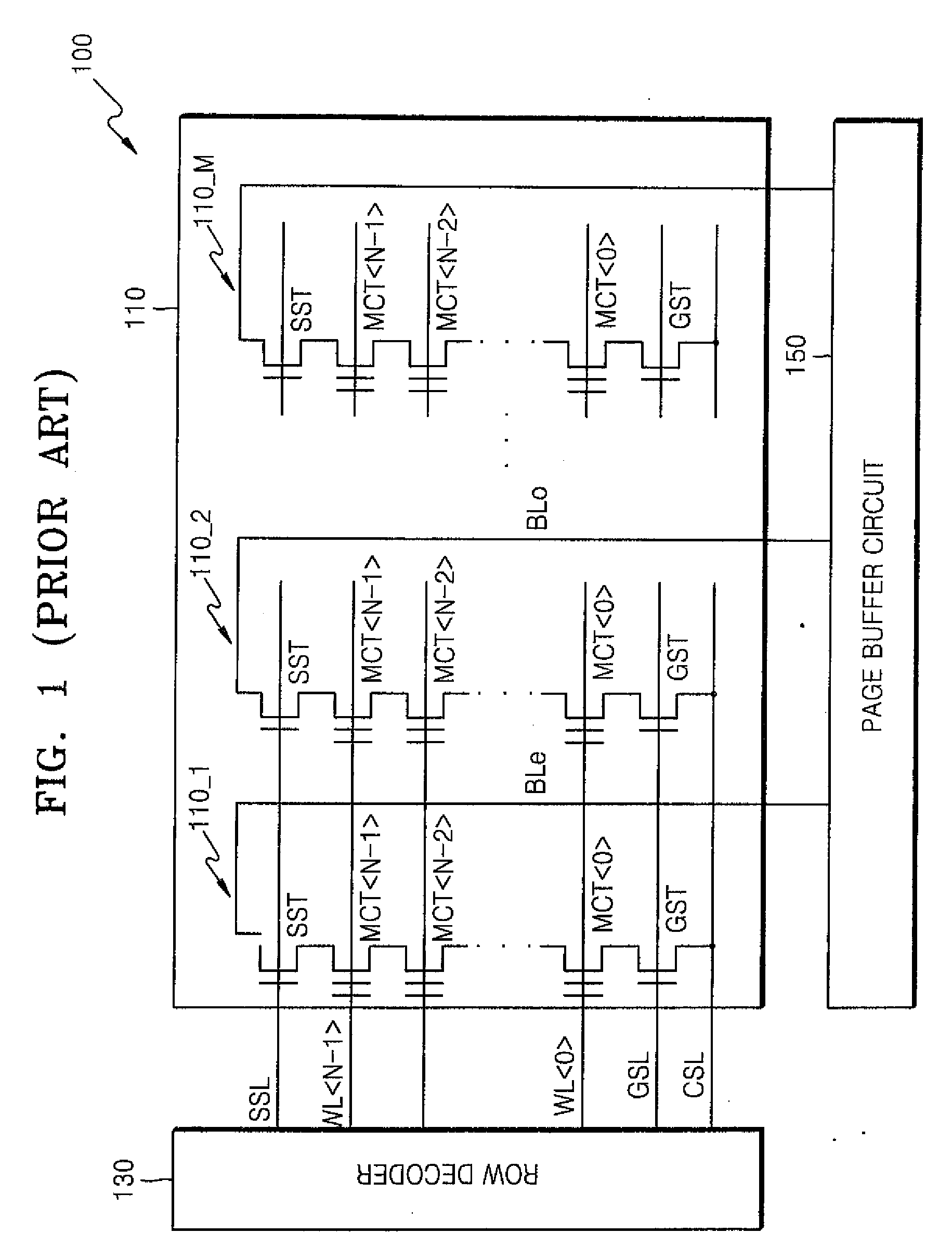
[0015]Exemplary embodiments of the present invention are directed to a method of programming a nonvolatile memory device. In an exemplary embodiment, the programming method employs hybrid boosting using both self-boosting and local boosting. The nonvolatile memory device includes a plurality of cell strings each having a plurality of electrically erasable and programmable memory cells connected in series and a plurality of wordlines respectively connected to control gates of the plurality of memory cells. The method includes receiving an address of a selected one of the plurality of memory cells to be programmed. A determination is made whether or not a selected wordline connected to the selected cell is located above or under a reference wordline based on the received address. The selected cell is programmed in a local boosting manner when the selected wordline corresponds to the reference wordline or is located above the reference wordline. The selected cell is programmed in a self-boosting manner when the selected wordline is located under said reference wordline.

Problems solved by technology

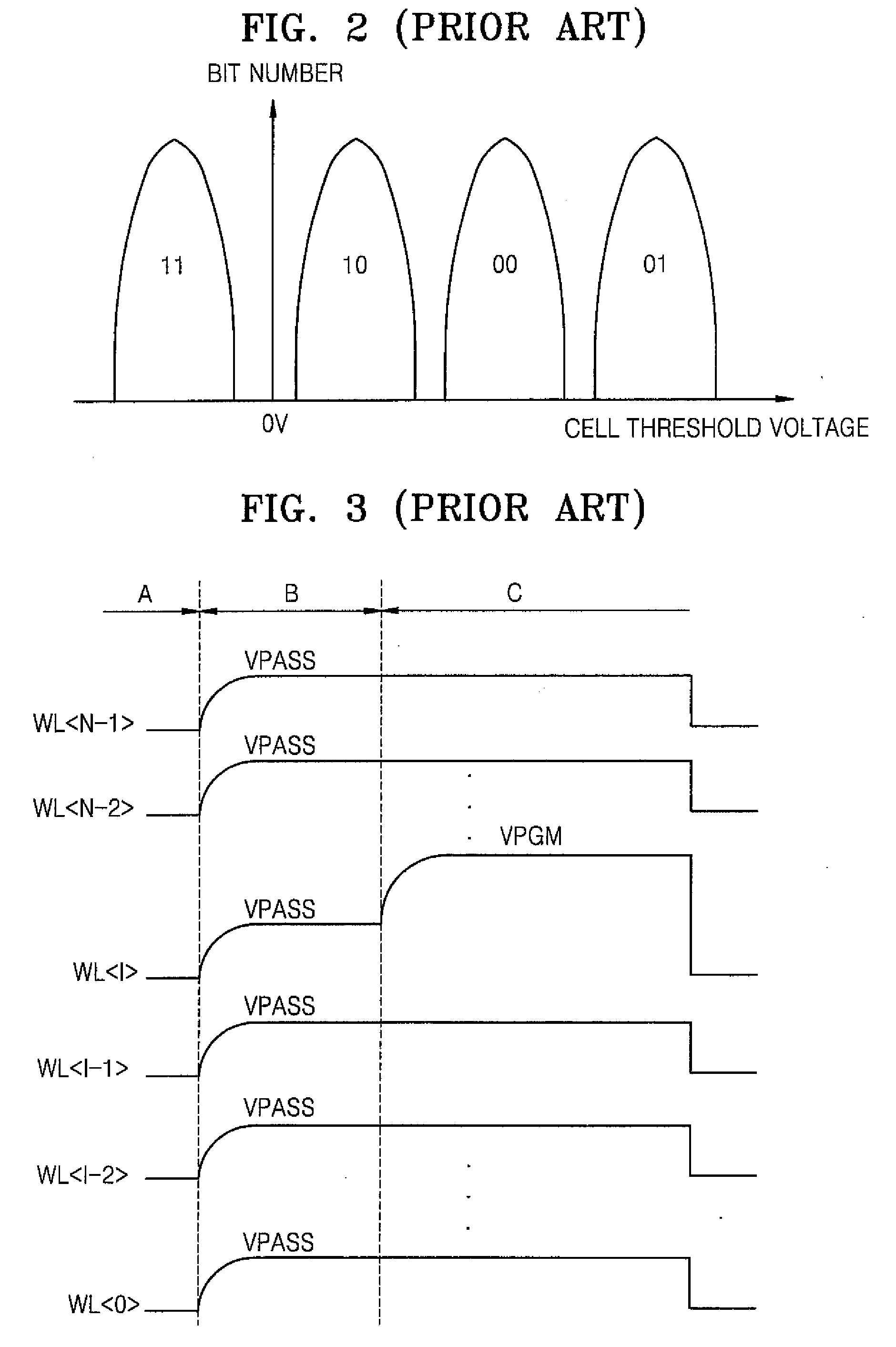
Particularly, when programming is performed from lower cells to upper cells, the program disturbance is aggravated when a selected cell is close to the upper cells because the number of cells bringing about charge sharing is increased.

Method used


Image

  • Method of programming a nonvolatile memory device using hybrid local boosting
  • Method of programming a nonvolatile memory device using hybrid local boosting
  • Method of programming a nonvolatile memory device using hybrid local boosting

Examples


Embodiment Construction

[0027]The present invention will now be described more fully hereinafter with reference to the accompanying drawings, in which preferred embodiments of the invention are shown. This invention, however, may be embodied in many different forms and should not be construed as limited to the embodiments set forth herein. Rather, these embodiments are provided so that this disclosure will be thorough and complete, and will fully convey the scope of the invention to those skilled in the art. In the drawings, like numbers refer to like elements throughout.

[0028]FIG. 6 is a timing diagram for explaining the local boosting method. Local voltage VLOCAL is applied to wordline WL1> connected to a cell directly under a programmed cell (i.e. a cell connected to a wordline WL). The wordline WL1> to which the local voltage is applied is operated in connection with wordline WL to which the program voltage is applied. Although FIG. 6 depicts local voltage VLOCAL applied to wordline WL1> connected to t...


PUM


Abstract

A method of programming a nonvolatile memory device using hybrid local boosting which includes a plurality of cell strings each having a plurality of electrically erasable and programmable memory cells connected in series and a plurality of wordlines respectively connected to control gates of the plurality of memory cells. The address of a selected cell that is to be programmed is received. A determination is made as to whether a selected wordline connected to the selected cell is located above or under a reference wordline based on the received address. The selected cell is programmed using local boosting when the selected wordline corresponds to the reference wordline or is located above the reference wordline. The selected cell is programmed using self-boosting when the selected wordline is located under the reference wordline. The programming method reduces circuit size of a nonvolatile memory device employing the programming method and efficiently prevents program disturbance due to charge sharing.

Description

CROSS-REFERENCE TO RELATED APPLICATION[0001]This U.S. non-provisional patent application claims priority under 35 U.S.C. §119 of Korean Patent Application No. 10-2006-006997 filed on Jul. 25, 2006, the entire contents of which are hereby incorporated by reference.BACKGROUND OF THE INVENTION[0002]1. Field of the Invention[0003]Embodiments of the invention relate to a method of programming a nonvolatile memory device. More particularly, embodiments of the invention relate to a method of programming a nonvolatile memory device through hybrid boosting using both self-boosting and local boosting.[0004]2. Discussion of Related Art[0005]A nonvolatile memory device, for example a flash memory, is electrically erasable and programmable and can preserve data even in the absence of power. One type of flash memory is a NAND type which has a string structure in which a plurality of flash memory cells is connected in series. NAND type flash memories can be easily integrated in and supplied at a l...

Claims


Application Information

Patent Timeline
Patent Type & Authority Applications(United States)
IPC IPC(8): G11C16/04G11C16/06
CPCG11C11/5628G11C16/0483G11C16/3427G11C16/30G11C16/3418G11C16/08G11C16/10G11C16/32
Inventor BYEON, DAE-SEOKLIM, YOUNG-HO
Owner SAMSUNG ELECTRONICS CO LTD
Learn More