

Vertical stack type multi-chip package having improved grounding performance and lower semiconductor chip reliability
a multi-chip, vertical stack technology, applied in the direction of semiconductor devices, semiconductor/solid-state device details, electrical apparatus, etc., can solve the problems of reducing the reliability of semiconductor devices, and achieve the effects of improving the reliability of lower semiconductor chips, improving grounding performance, and increasing the siz
- Summary
- Abstract
- Description
- Claims
- Application Information
AI Technical Summary
Benefits of technology
Problems solved by technology
Method used
Image

Examples
Embodiment Construction
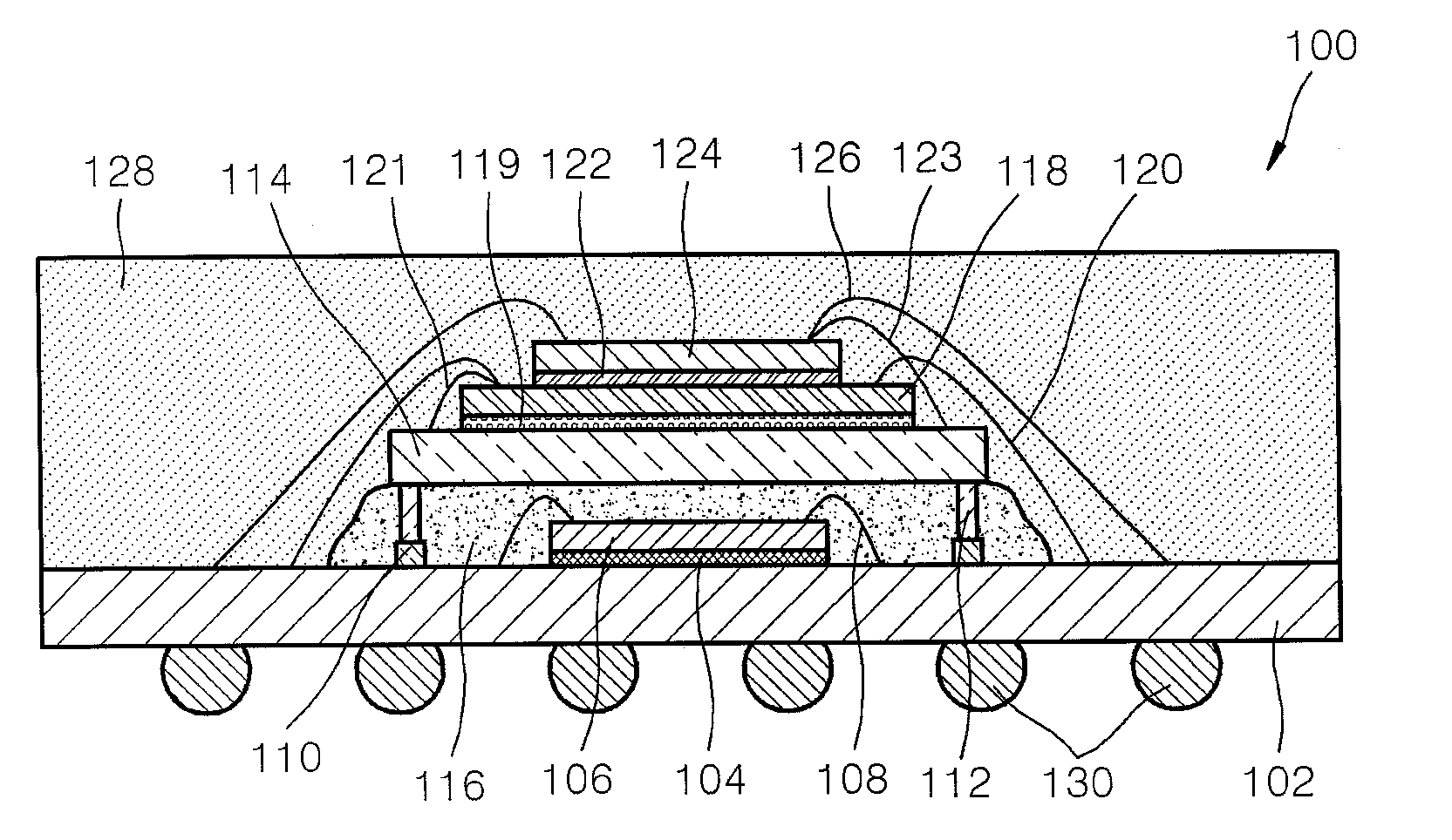
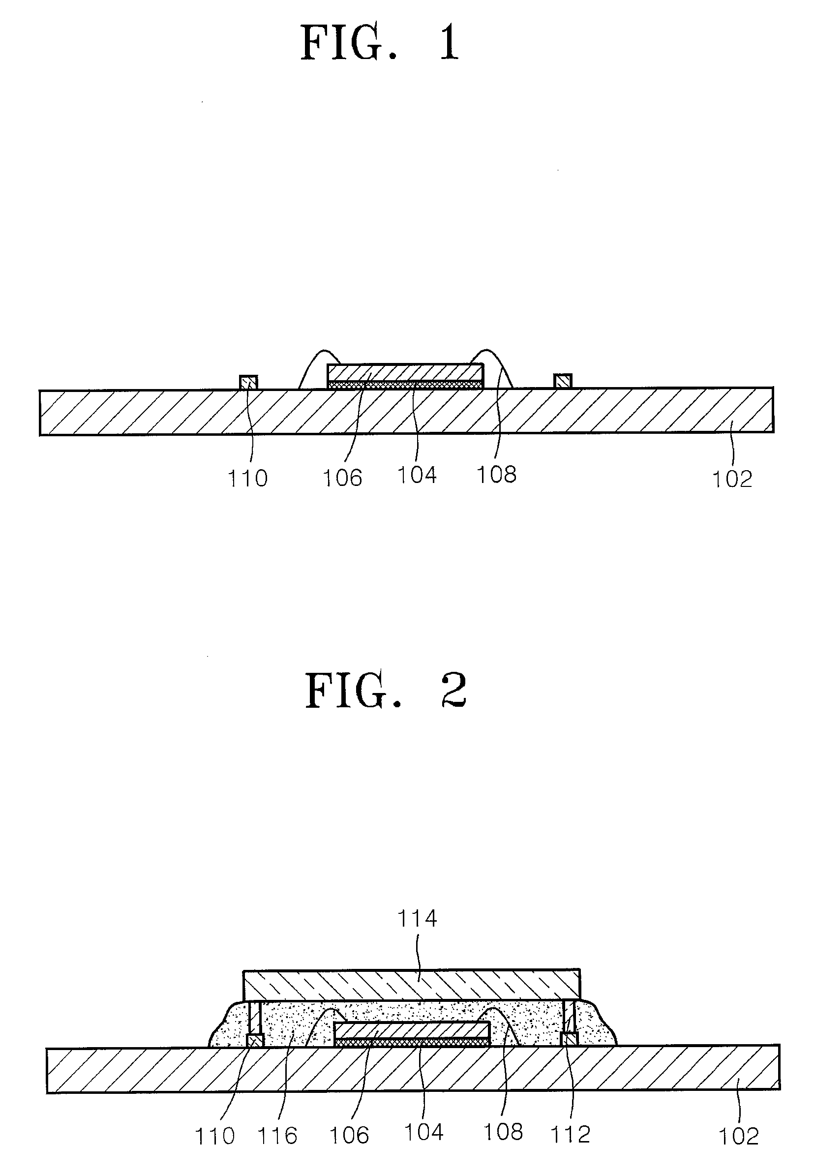
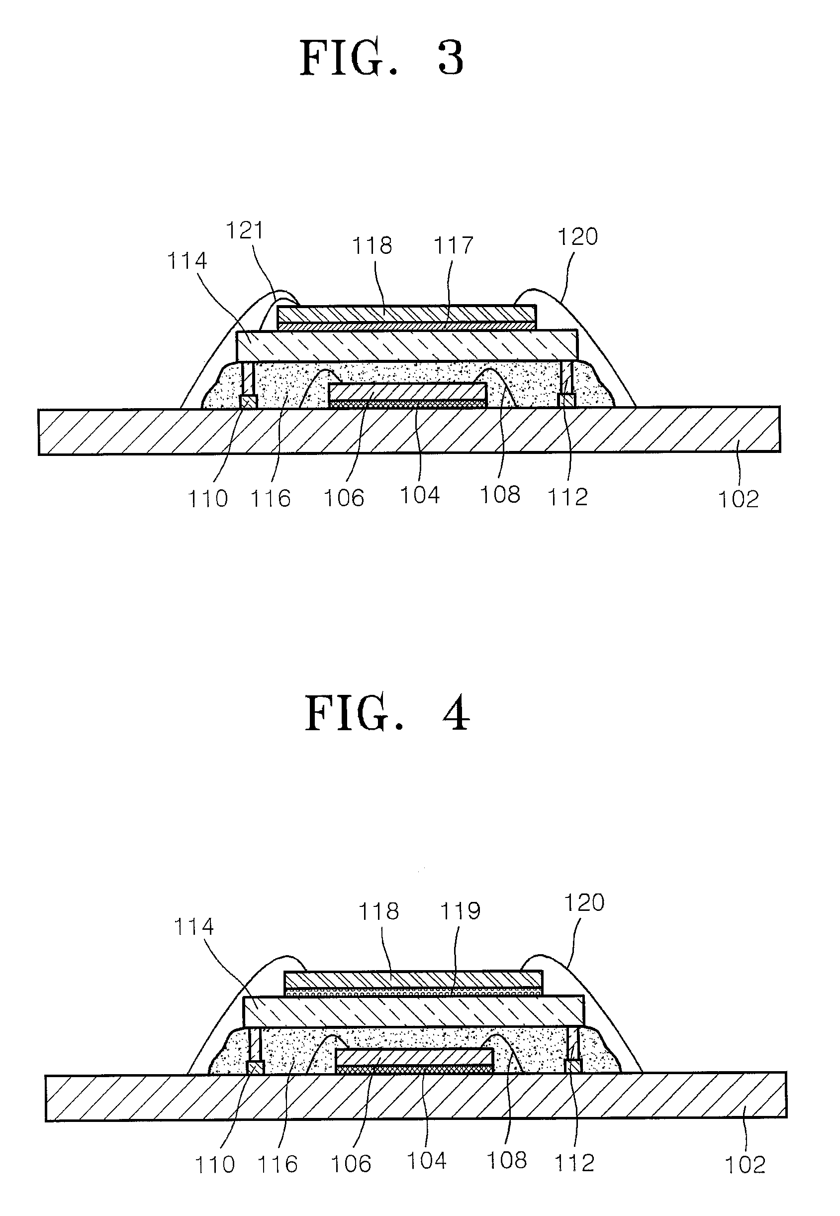
[0016]The present invention will now be described more fully hereinafter with reference to the accompanying drawings, in which preferred embodiments of the invention are shown. This invention may, however, be embodied in many different forms and should not be construed as being limited to the embodiments set forth herein. Rather, these embodiments are provided so that this disclosure will be thorough and complete, and will fully convey the scope of the invention to those skilled in the art. For example, an organic substrate has been used as a main frame of a semiconductor package in the embodiment of the present invention, but the main frame may be replaced with a conventional main frame for a semiconductor package such as a lead frame.
[0017]FIG. 1 is a sectional view illustrating a semiconductor chip 106 mounted on an organic substrate 102 using a die bonding material 104. Semiconductor chip 106 may be a device used for radio frequency (RF) applications, which is relatively small i...
PUM
 Abstract
Description
Claims
Application Information