Magnetic sensor circuit, semiconductor device, and magnetic sensor device

a technology of magnetic sensor and semiconductor device, which is applied in the direction of magnetic measurement, measurement device, instruments, etc., can solve the problems of preventing satisfactory execution of offset cancellation, difficult to realize, and not achieving perfectly differential operation

Inactive Publication Date: 2008-02-07
ROHM CO LTD
View PDF0 Cites 42 Cited by
  • Summary
  • Abstract
  • Description
  • Claims
  • Application Information

AI Technical Summary

Benefits of technology

[0023] It is an object of the present invention to provide a magnetic sensor circuit that includes a magnetism detection circuit adopting a differential circuit configuration, that is less affected by the device offset voltage appearing in a magnetoelectric conversion device such as a Hall device or magnetic resisti

Problems solved by technology

In reality, however, the combination of the capacitor 4 and the voltage amplifier 3 does not promise perfectly differential operation.
As a result, for example, delay (bluntness) caused by the capacitor 4, or ripples or noise in the supply voltage, may prevent satisfactory execution of offset cancellation.
Inconveniently, this makes it diff

Method used


Image

  • Magnetic sensor circuit, semiconductor device, and magnetic sensor device
  • Magnetic sensor circuit, semiconductor device, and magnetic sensor device
  • Magnetic sensor circuit, semiconductor device, and magnetic sensor device

Examples


first embodiment

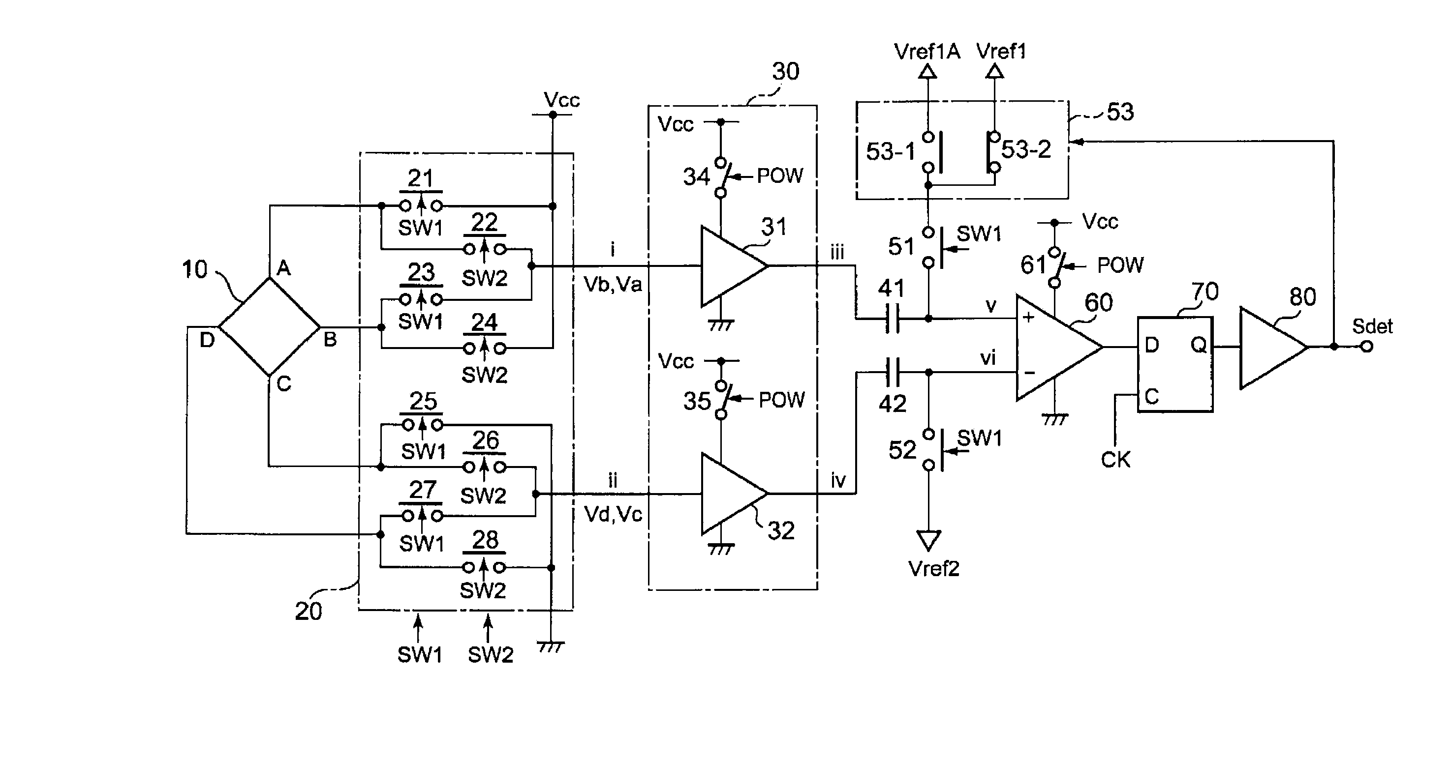
[0038] FIGS. 1 to 5 are diagrams showing the configuration of a magnetic sensor circuit according to a first embodiment of the present invention. This embodiment is one which the applicant of the present invention already proposed in Japanese Patent Application No. 2005-230781 (a domestic application claiming the priority date based on a prior domestic application No. 2005-031715). In FIG. 1, as in the conventional example shown in FIG. 11, a Hall device is formed as a plate having a shape that is geometrically equivalent with respect to four terminals A, C, B, and D.

[0039] In this Hall device 10, between the Hall voltage that appears across a second pair of terminals (B and D) when the supply voltage Vcc is applied across a first pair of terminals (A and C) and the Hall voltage that appears across the first pair of terminals (C and A) when the supply voltage Vcc is applied across a second pair of terminals (B and D), the effective signal components contained respectively in them—t...

second embodiment

[0085]FIG. 6 is a diagram showing the configuration of a magnetic sensor circuit according to a second embodiment of the present invention.

[0086] The magnetic sensor circuit according to the second embodiment includes a first Hall device 10X, a second Hall device 10Y, a first selection switch circuit 20X, a second selection switch circuit 20Y, a first amplifier unit 30X, a second amplifier unit 30Y, a first capacitor 41X, a second capacitor 42X, a third capacitor 41Y, a fourth capacitor 42Y, a first switch circuit 51, a second switch circuit 52, a reference voltage switch circuit 53, a comparison unit 60, a latch circuit 70, a buffer amplifier 80, a reference voltage generation circuit 90, and a control circuit 100.

[0087] The first Hall device 10X generates, across a first pair of terminals (A and C) or across a second pair of terminals (B and D), an output voltage commensurate with the magnetism applied to it.

[0088] The second Hall device 10Y is arranged side by side with the fi...

third embodiment

[0115]FIG. 9 is a diagram showing the configuration of a magnetic sensor circuit according to a third embodiment of the present invention.

[0116] As shown in FIG. 9, the magnetic sensor circuit according to the third embodiment includes, instead of the first and second amplifier units 30X and 30Y of the two-input, two-output type, a first and a second amplifier unit 30X′ and 30Y′ of the two-input, one-output type. The first amplifier unit 30X′ amplifies with a predetermined amplification factor a the difference between the voltage appearing at a first output terminal I and fed to a first amplification input terminal (+) and the voltage appearing at a second output terminal II and fed to a second amplification input terminal (−) to output a first amplified voltage to a first amplification output terminal (+). The second amplifier unit 30Y′ amplifies with the predetermined amplification factor α the difference between the voltage appearing at a third output terminal III and fed to a t...


PUM


Abstract

A magnetic sensor circuit has Hall devices 10X and 10Y, selection switch circuits 20X and 20Y, amplifier units 30X ad 30Y, a comparison unit 60, capacitors 41X, 42X, 41Y, and 42Y, and switch circuits 51 and 52. The Hall voltages obtained from the Hall devices 10X and 10Y are outputted in either of a first and a second states switched by the selection switch circuits 20X and 20Y. The amplifier units 30X ad 30Y each operate differentially and, if the difference between their outputs is greater than a set hysteresis width, the output logic of a detection signal Sdet is shifted. This configuration helps reduce the influence of device offset voltages in the Hall devices, and also helps reduce the influence of input offset voltages arising in the amplifiers.

Description

[0001] This application is based on Japanese Patent Application No. 2006-203592 filed on Jul. 26, 2006, the contents of which are hereby incorporated by reference. BACKGROUND OF THE INVENTION [0002] 1. Field of the Invention [0003] The present invention relates to a magnetic sensor circuit that amplifies with an amplifier an output voltage of a Hall device, magnetic resistive device, or the like to detect magnetism at the site at which it is placed, in order to output a magnetism detection signal. The present invention also relates to a semiconductor device having such a magnetic sensor circuit integrated into it, and to a magnetic sensor device employing such a semiconductor device. [0004] 2. Description of Related Art [0005] Typically, a magnetic sensor circuit comprises a Hall device that outputs an output voltage proportional to the intensity of a magnetic field, an amplifier that amplifies the output voltage of the Hall device, and a comparator that compares the output voltage ...

Claims


Application Information

Patent Timeline
IPC IPC(8): G01R33/02
CPCG01R33/07
Inventor NISHIKAWA, HIDETOSHI
Owner ROHM CO LTD
Why Eureka
Try Eureka