Systems and Methods for Continuity Testing Using a Functional Pattern

a technology of functional pattern and system, applied in the direction of electrical testing, measurement device, instruments, etc., can solve the problems of device under test failure, etc., and achieve the effect of high speed

Active Publication Date: 2008-02-07
TEXAS INSTR INC
View PDF5 Cites 20 Cited by
  • Summary
  • Abstract
  • Description
  • Claims
  • Application Information

AI Technical Summary

Benefits of technology

[0006]In some instances of the aforementioned embodiments, the test pin node is electrically coupled to a pin of a device under test. In such instances, the methods may further include applying a first voltage to the threshold voltage input, and a second voltage to the threshold comparator input. In some cases where the second voltage is greater than the first voltage, the methods may include sensing an output of the comparator. In such cases where it is detected that a voltage at the test pin node is less than the second voltage, the device under test is failed for lack of continuity. As one particular example, the device under test may include a ground diode electrically coupling the pin of the device under test to ground, a first voltage of approximately negative 2V, and a second voltage of approximately negative 1.1V. In such a case, where sensing the output of the comparator indicates a voltage at the test pin node that is less than the second voltage, the device under test is failed for lack of continuity between the pin of the device under test and ground via the ground diode.
[0007]In some cases of the aforementioned embodiments where the second voltage is greater than the first voltage, another pin associated with the device under test may be driven with a third voltage. In such a case, the output of the comparator may be sensed and it may be determined that a voltage at the test pin node is greater than the second voltage. In such a case, the device under test is failed for a short between the first pin and the second pin or between the first pin and ground. As one particular example, one pin of the device under test may be driven with a third voltage that is approximately positive 0.3V, the first voltage is approximately negative 2.0V, and the second voltage is approximately negative 0.3V. In such a case, the device under test is failed for a short between the two pins where the output of the comparator indicates that the voltage at the test pin node greater than the second voltage is detected.
[0008]In other cases of the aforementioned instances where the second voltage is less than the first voltage, the methods may further include sensing the output of the comparator and determining that the device fails for lack of continuity where the output of the comparator indicates that the voltage at the test pin node is greater than the second voltage. As one particular example, the device under test includes a VCC diode electrically coupling the pin of the device under test to VCC, the first voltage is approximately positive 2V, and the second voltage is approximately positive

Problems solved by technology

In such cases where it is detected that a voltage at the test pin node is less than the second voltage, the device under test is failed for lack of continuity.
In such a case, where sensing the output of the comparator indicates a voltage at the test pin node that is less than the

Method used


Image

  • Systems and Methods for Continuity Testing Using a Functional Pattern
  • Systems and Methods for Continuity Testing Using a Functional Pattern
  • Systems and Methods for Continuity Testing Using a Functional Pattern

Examples


Embodiment Construction

[0018]The present invention is related to systems and methods for testing semiconductor devices, and in particular to systems and methods for testing semiconductor devices using a functional pattern.

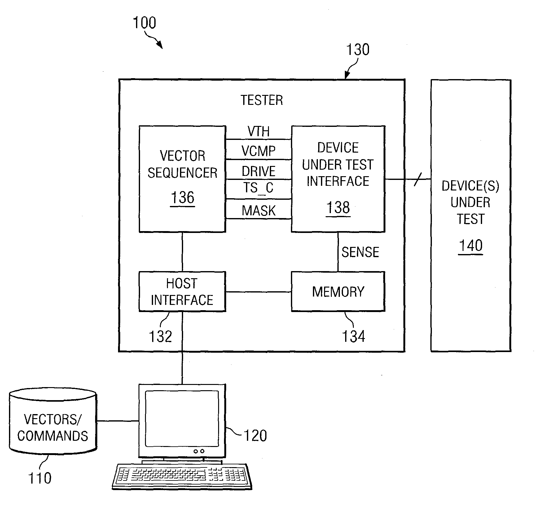
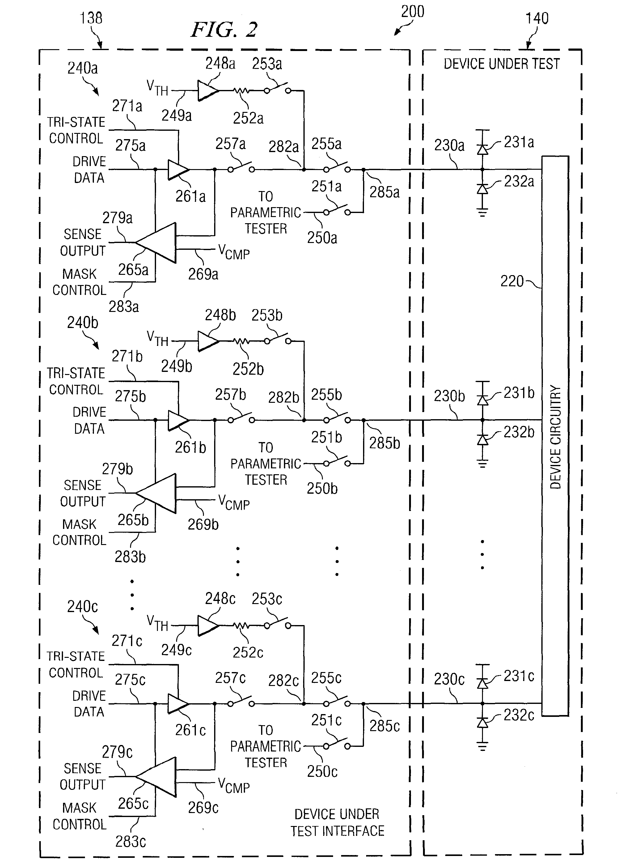
[0019]Turning to FIG. 1, a tester set-up 100 that may be employed in relation to various embodiments of the present invention is depicted. Tester set-up 100 includes a microprocessor based machine 120 that is associated with a computer readable medium 110, and a tester 130. Microprocessor based machine 120 may be any microprocessor based machine such as, for example, a personal computer that is communicably coupled to tester 130. Alternatively, microprocessor based machine may consist essentially of a processor that is incorporated directly into tester 130. Based on the disclosure provided herein, one of ordinary skill in the art will recognize a number of microprocessor based machines and / or processors that may be used in relation to one or more embodiments of the present invention. Com...


PUM


Abstract

Various systems and methods for device configuration are disclosed herein. For example, some embodiments of the present invention provide high speed pin continuity and pin-to-pin short tester circuits. Such circuits include a threshold driver, a test driver, and a comparator. An input of the threshold driver is electrically coupled to a voltage threshold, and an output of the threshold driver is electrically coupled to a test pin node via a current limiting resistor. An input of the test driver is electrically coupled to a drive data input, and an output of the test driver is electrically coupled to the test pin node. One input of the comparator is electrically coupled to the test pin node, and the other input of the comparator is electrically coupled to a threshold comparator input.

Description

BACKGROUND OF THE INVENTION[0001]The present invention is related to systems and methods for testing semiconductor devices, and in particular to systems and methods for testing semiconductor devices using a functional pattern.[0002]It is common for semiconductor devices to be inoperable at the end of the manufacturing process due to one or more manufacturing errors. For this reason, various tests are performed on semiconductor devices at the end of the manufacturing process and / or at interim points in the manufacturing process. For example, one existing method provides for testing each pin for continuity by serially testing one pin at a time using a parametric tester. Subsequently, each pin is serially tested for shorts to one or more of the other pins of the semiconductor device using the same parametric tester. Such an approach is effective for determining proper device connectivity, however, the approach is time consuming. Such time consumption in the testing phase of the semicon...

Claims


Application Information

Patent Timeline
IPC IPC(8): G01R31/26
CPCG01R31/31924G01R31/31932G01R31/31928
Inventor PATEL, GUNVANT T.TARSI, TREVOR J.WANG, YUNG-FULENDINO, ANTHONY J.
Owner TEXAS INSTR INC
Why Eureka
Try Eureka