

Methods and systems for controlling critical dimensions in track lithography tools
a technology of critical dimensions and track lithography, applied in the direction of hot plate heating arrangement, semiconductor/solid-state device testing/measurement, instruments, etc., can solve the problems of reliability problems and adversely affect the yield of devices, and achieve the effect of improving cd uniformity
- Summary
- Abstract
- Description
- Claims
- Application Information
AI Technical Summary
Benefits of technology
Problems solved by technology
Method used
Image

Examples
Embodiment Construction
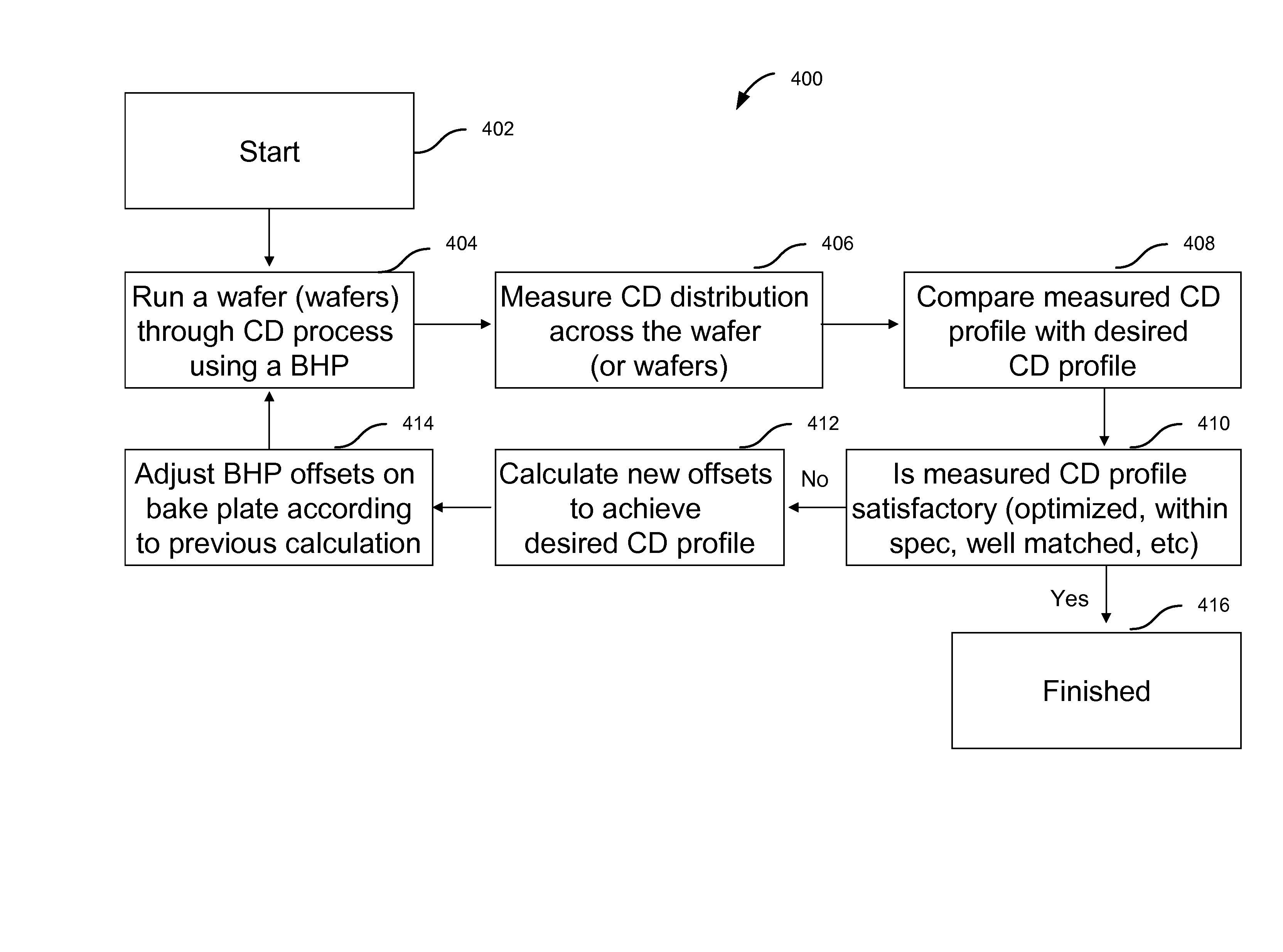
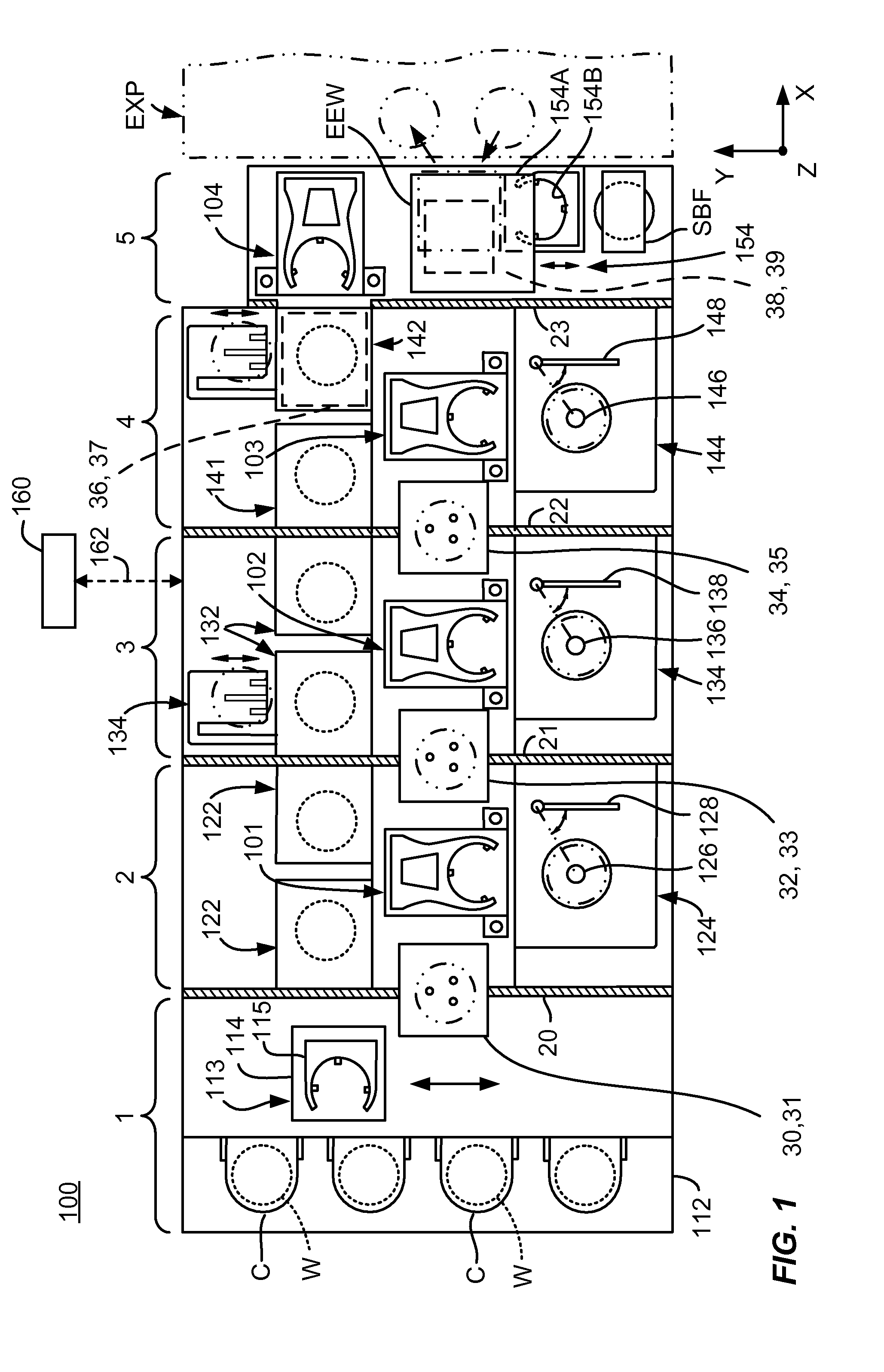
[0032]FIG. 1 is a plan view of a track lithography tool according to an embodiment of the present invention. In the embodiment illustrated in FIG. 1, the track lithography tool is coupled to an immersion scanner. An XYZ rectangular coordinate system in which an XY plane is defined as the horizontal plane and a Z axis is defined to extend in the vertical direction is additionally shown in FIG. 1 for purposes of clarifying the directional relationship therebetween.
[0033] In a particular embodiment, the track lithography tool is used to form, through use of a coating process, an anti-reflection (AR) and a photoresist film on substrates, for example, semiconductor wafers. The track lithography tool is also used to perform a development process on the substrates after they have been subjected to a pattern exposure process. Additional processes performed on the track lithography tool, which may be coupled to an immersion scanner, include PEB and the like. The substrates processed by the ...
PUM
 Abstract
Description
Claims
Application Information