Method of manufacturing semiconductor device that includes forming self-aligned contact pad

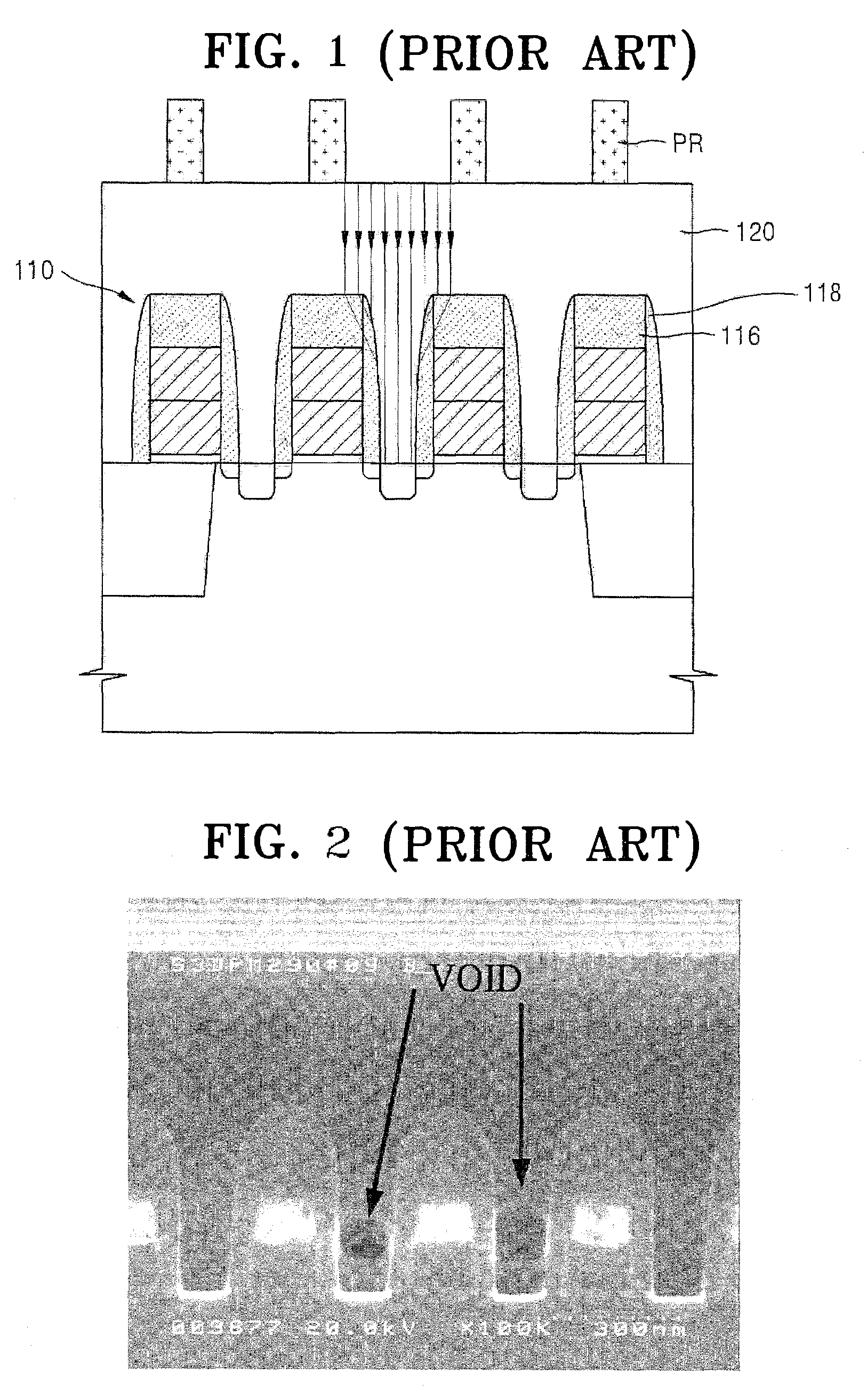
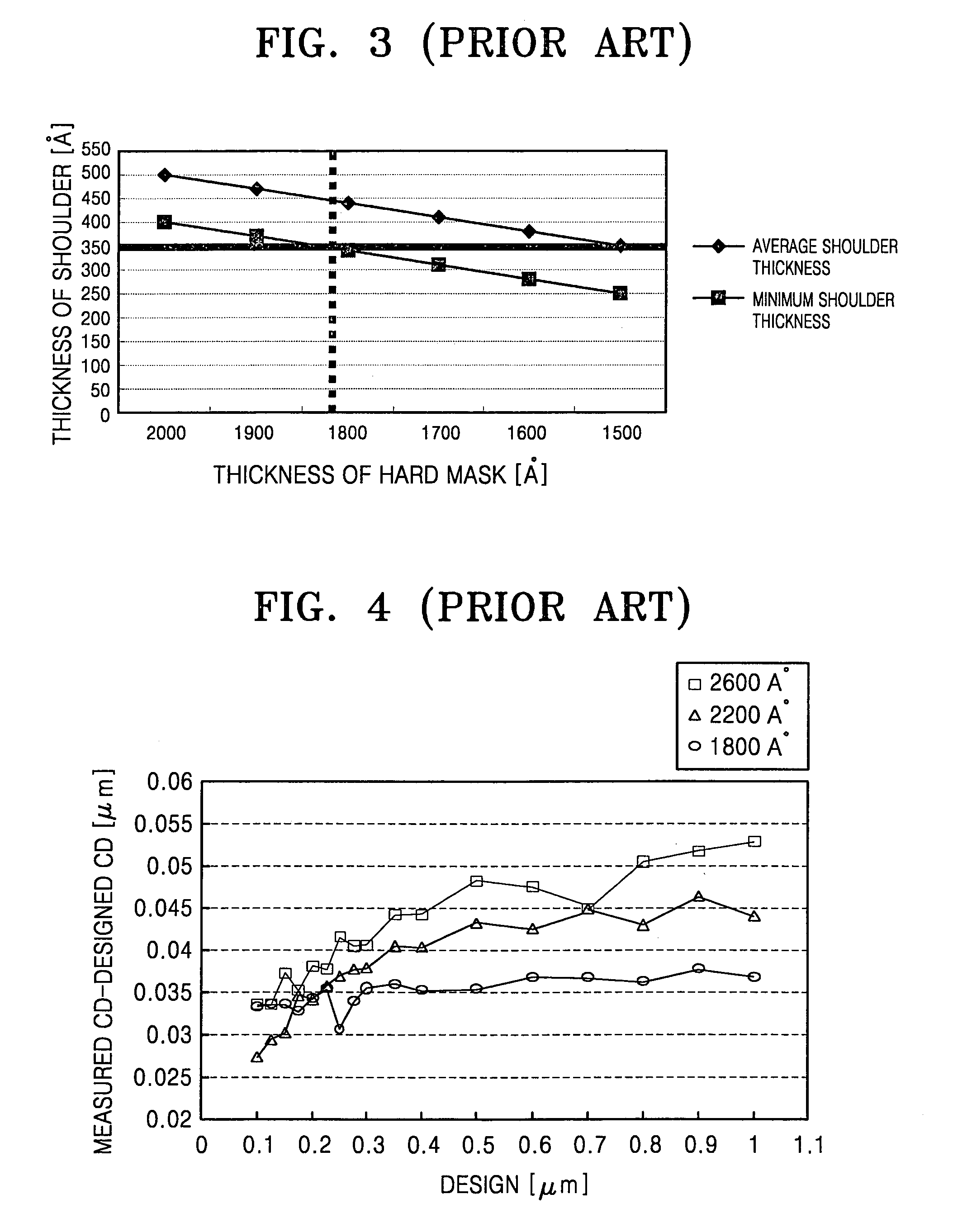
a technology of contact pads and semiconductor devices, which is applied in the direction of semiconductor devices, basic electric elements, electrical appliances, etc., can solve the problems of reducing voids or similar imperfections, and the difficulty of completely filling the interlayer insulating material between the gate electrode structures, etc., to achieve the effect of facilitating the gap filling, lowering the height and improving the cd profile of the gate electrode structur

Inactive Publication Date: 2007-08-07
SAMSUNG ELECTRONICS CO LTD
View PDF5 Cites 15 Cited by
  • Summary
  • Abstract
  • Description
  • Claims
  • Application Information

AI Technical Summary

Benefits of technology

[0019]Some embodiments provide a method of manufacturing a semiconductor device including an SAC pad forming process, which facilitates the gap filling by an interlayer insulating layer by lowering the height of the gate electrode structure, improves the CD profile of the gate electrode structure, and enhances CD uniformity of the gate electrode structure.
[0020]Some embodiments also provide a method of manufacturing a semiconductor device including an SAC pad forming process, which prevents a short-circuit between the SAC pad and a gate conductive film in spite of a decrease in the thickness of the hard mask and prevents a middle bridge from being generated.

Problems solved by technology

The increase in the aspect ratio of the gate electrode structure makes it difficult to completely fill the interlayer insulating material between the gate electrode structures.
If the gap filling characteristic of the interlayer insulating layer is poor, voids or similar imperfections are generated in the interlayer insulating layer.
To prevent voids, it is necessary to reduce the height of the gate electrode structure, which is limited.
However, this method cannot be a realistic alternative because it reduces the surface area of the gate conductive film resulting in an increase of the resistance of the gate line.
However, this method also has a limitation related to the SAC pad forming process.
As aforementioned, to ensure the shoulder of the gate electrode structure has a sufficient thickness after the self-aligned etch process, the thickness of the hard mask and the thickness of the spacer should be thick, and therefore, there is a limitation in reducing the thickness of the hard mask and the thickness of the spacer.
Accordingly, there is a limitation to increasing the thickness of the shoulder.
When using the conventional SAC pad forming process, it is not easy to decrease the thickness of the hard mask below 2000 Å, so there is a limitation in reducing the aspect ratio of the gate electrode structure.
As the overall height of the gate electrode structure increases, another problem, i.e., deterioration of the critical dimension (CD) uniformity of the gate electrode structure may occur.
The increase in the deviation between the CDs means that the uniformity of the CD becomes worse with respect to the position of the line as well as on the same line.
If the uniformity of the CD becomes worse, the linearity of the gate electrode structure becomes worse, and it is difficult to obtain a gate electrode structure having a desired shape.
If the measurement CD is smaller than the design CD, the refresh characteristics of the DRAM device may be deteriorated.
If the measurement CD is larger than the design CD, tRCD failure may occur.
Thus, if the CD uniformity is bad, the performance of the transistor may be deteriorated, thereby lowering the reliability of the semiconductor device.
As the design rule decreases and the height of the gate electrode structure increases, another problem, for example, a middle bridge, may occur.
However, as described later, if the photoresist pattern is not used as the etch mask, it is difficult to secure a process margin of the SAC hole etch process.

Method used


Image

  • Method of manufacturing semiconductor device that includes forming self-aligned contact pad
  • Method of manufacturing semiconductor device that includes forming self-aligned contact pad
  • Method of manufacturing semiconductor device that includes forming self-aligned contact pad

Examples


Embodiment Construction

[0034]The invention will now be described more fully with reference to the accompanying drawings, in which exemplary embodiments of the invention are shown. The invention may, however, be embodied in many different forms and should not be construed as being limited to the embodiments set forth herein; rather, these embodiments are provided so that this disclosure will be thorough and complete, and will fully convey the concept of the invention to those skilled in the art. In the drawings, the thickness of layers and regions are exaggerated for clarity. Like reference numerals in the drawings denote like elements, and thus their description will be omitted.

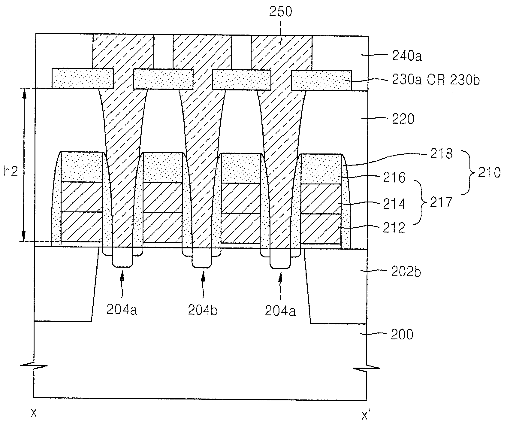
[0035]FIGS. 5A and 5B through FIG. 9 illustrate a method of manufacturing a semiconductor device including forming a SAC pad according to some embodiments of the invention.

[0036]FIG. 5A is a plan diagram illustrating an active region and a gate line stack of the semiconductor device, and FIG. 5B is a cross-sectional diagram taken a...


PUM


Abstract

According to some embodiments, a gate electrode structure including a gate electrode stack and a spacer, and source / drain region are formed on a semiconductor substrate. A first interlayer insulating layer having a thickness greater than that of the gate electrode structure is formed on the semiconductor substrate. On the first interlayer insulating layer, an etch inducing and focusing mask extending in a same direction as a length direction of the gate electrode structure and covering the gate electrode structure is formed. A second interlayer insulating layer is formed on the first interlayer insulating layer. A photoresist pattern is formed on the second interlayer insulating layer. The second interlayer insulating layer and the first interlayer insulating layer are sequentially etched using the photoresist pattern as an etch mask, thereby forming a SAC hole. A conductive material is used to fill in the SAC hole to form a SAC pad.

Description

CROSS REFERENCE TO RELATED APPLICATIONS[0001]This application claims priority from Korean Patent Application No. 2003-78897, filed on Nov. 8, 2003, in the Korean Intellectual Property Office, the content of which is incorporated by reference in its entirety for all purposes.BACKGROUND OF THE INVENTION[0002]1. Field of the Invention[0003]This disclosure relates to a method of manufacturing a semiconductor device, and more particularly, to a method of manufacturing a semiconductor device including a process of forming a self-aligned contact pad.[0004]2. Description of the Related Art[0005]Due to the reduction in the design rule of semiconductors, a Self-Aligned Contact (SAC) pad forming process has been added in the contact pad forming process. The SAC pad forming process uses a high etch selectivity between materials, thus securing a sufficient process margin in the exposure process and the etch process in spite of the reduction of the design rule. For instance, when forming an SAC h...

Claims


Application Information

Patent Timeline
Patent Type & Authority Patents(United States)
IPC IPC(8): H01L21/4763H01L21/28H01L21/302H01L21/311H01L21/336H01L21/60H01L21/8242
CPCH01L21/31144H01L21/76897H01L27/10855H01L27/10888H10B12/485H10B12/0335H01L21/28
Inventor HWANG, JAE-HEELEE, JEONG-YUNKIM, TAE-RYONGPARK, YONG-HYEON
Owner SAMSUNG ELECTRONICS CO LTD
Why Eureka
Try Eureka