Method for controlling pattern uniformity of semiconductor device

a semiconductor device and pattern technology, applied in the field of semiconductor devices, can solve the problems of difficult use of af, scum from the af itself, and difficulty in checking patterns, and achieve the effect of improving cd uniformity

Active Publication Date: 2011-11-10
SK HYNIX INC
View PDF5 Cites 0 Cited by
  • Summary
  • Abstract
  • Description
  • Claims
  • Application Information

AI Technical Summary

Benefits of technology

[0012]Embodiments of the present invention are directed to a method for improving CD uniformity on a wafer and a process margin (e.g., depth of focus (DOF) margin) by controlling a size of an outermost pattern among target patterns.

Problems solved by technology

However, as the semiconductor device becomes highly integrated and a design rule has been rapidly reduced, various problems occur due to a resolution limit of the photolithography process.
However, as the semiconductor devices have become ultra dense, it is not easy to use the AF because of the following restrictions.
Conversely, if the AF is located too close to the main pattern to maximize the interference effect, scum can occur from the AF itself.
The photo-mask maker, however has difficulties in checking the patterns if the pattern size is less than 40 nm.
However, most of the AF causes scum on a wafer.
However, the photo-mask maker has difficulty checking this pattern size so may not be able to check an optimal AF pattern size that is suitable for the ArF process.

Method used


Image

  • Method for controlling pattern uniformity of semiconductor device
  • Method for controlling pattern uniformity of semiconductor device
  • Method for controlling pattern uniformity of semiconductor device

Examples


Embodiment Construction

[0025]The present invention relates to a method for improving critical dimension (CD) uniformity of inner patterns by controlling an outermost pattern or plural outer patterns among target patterns without inserting an AF or changing design with respect to a layout of patterns. As used herein, the inner patterns refer to patterns other than the outermost pattern or the plural outer patterns among the target patterns.

[0026]Embodiments of the present invention are described in detail with reference to the accompanying drawings.

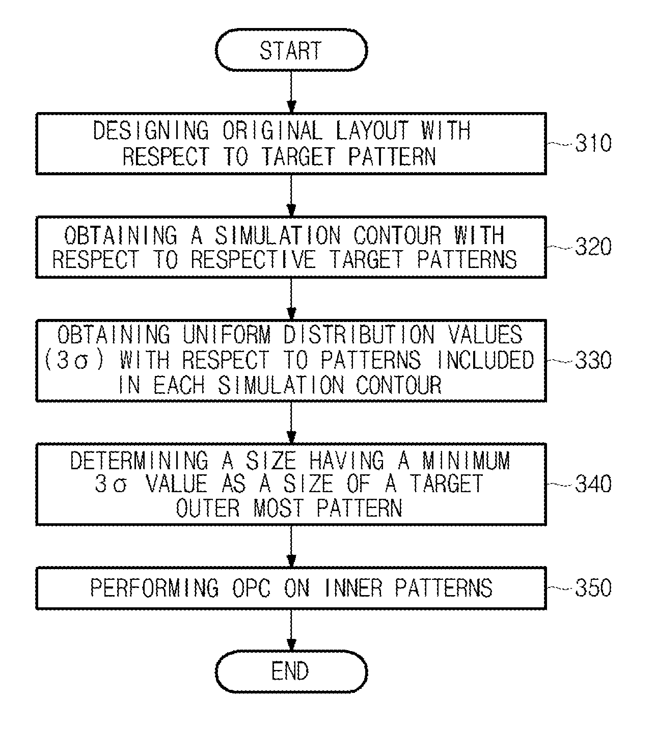
[0027]FIG. 3 is a flowchart illustrating a method for controlling pattern uniformity of a semiconductor device according to an embodiment of the present invention.

[0028]An original layout with respect to target patterns is designed (step 310).

[0029]At this time, the original layout is a mask layout. For example, the original layout may be a layout of patterns having a uniform size, and the patterns are formed at predetermined intervals. The pattern may include a...


PUM

PropertyMeasurementUnit
sizeaaaaaaaaaa
sizeaaaaaaaaaa
space sizeaaaaaaaaaa

Abstract

A method for controlling uniformity of patterns formed in a semiconductor device includes obtaining simulation contours with respect to respective cases while controlling a size of an outermost pattern and determining a size of the outermost pattern in which uniform distribution values (3σ) value of patterns included in the simulation contours satisfying specific conditions as a size of target outermost pattern.

Description

CROSS-REFERENCES TO RELATED APPLICATIONS[0001]The priority of Korean patent application No. 10-2010-0043035 filed on May 7, 2010, the disclosure of which is hereby incorporated in its entirety by reference, is claimed.BACKGROUND OF THE INVENTION[0002]The present invention relates to a semiconductor device, and more particularly, to a method for controlling uniformity of patterns formed in a semiconductor device.[0003]Generally, photolithography is a technology for creating high integration semiconductor devices by forming patterns in a predetermined shape on a wafer substrate using light. Namely, light (e.g., an ultraviolet ray, an electron beam, or an X ray) is irradiated onto a photoresist layer where a predetermined portion of the photoresist layer is exposed to the light using a photo-mask. Then a part of the photoresist layer having large solubility with respect to a developing solution is removed to form a photoresist pattern in a predetermined shape. The part of the layer (un...

Claims


Application Information

Patent Timeline
Patent Type & Authority Applications(United States)
IPC IPC(8): G06F17/50G03F1/36G03F1/68H01L21/027
CPCG03F1/36
Inventor HAN, DUK SUNKIM, MI HYE
Owner SK HYNIX INC
Why Eureka
Try Eureka