Image sensor having improved sensitivity and method of manufacturing the same

a technology of image sensor and manufacturing method, which is applied in the field of image sensor, can solve the problems of reducing the sensitivity of the photoelectric conversion element, affecting the sensitivity of the image sensor, and requiring a large investment in fabrication equipment, so as to achieve the effect of improving the sensitivity

Inactive Publication Date: 2008-02-14
SAMSUNG ELECTRONICS CO LTD
View PDF4 Cites 32 Cited by
  • Summary
  • Abstract
  • Description
  • Claims
  • Application Information

AI Technical Summary

Benefits of technology

[0010]Embodiments of the present invention are directed to an image sensor having improved sensitivity, even when employing aluminum interconnect

Problems solved by technology

Power consumption is also low; therefore such sensors can be applied to products where battery capacity is limited.
When aluminum interconnecting wires are used as described above, the vertical distance from a photoelectric conversion element, formed in a substrate, to an uppermost micro-lens at a top of the structure is

Method used


Image

  • Image sensor having improved sensitivity and method of manufacturing the same
  • Image sensor having improved sensitivity and method of manufacturing the same
  • Image sensor having improved sensitivity and method of manufacturing the same

Examples


Embodiment Construction

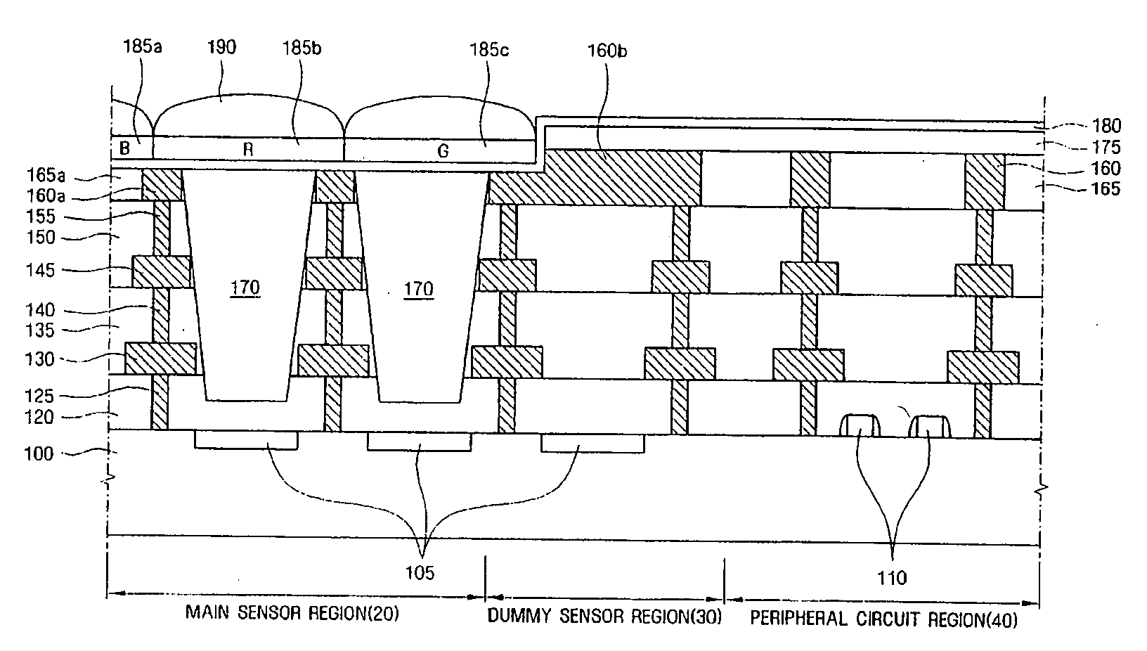
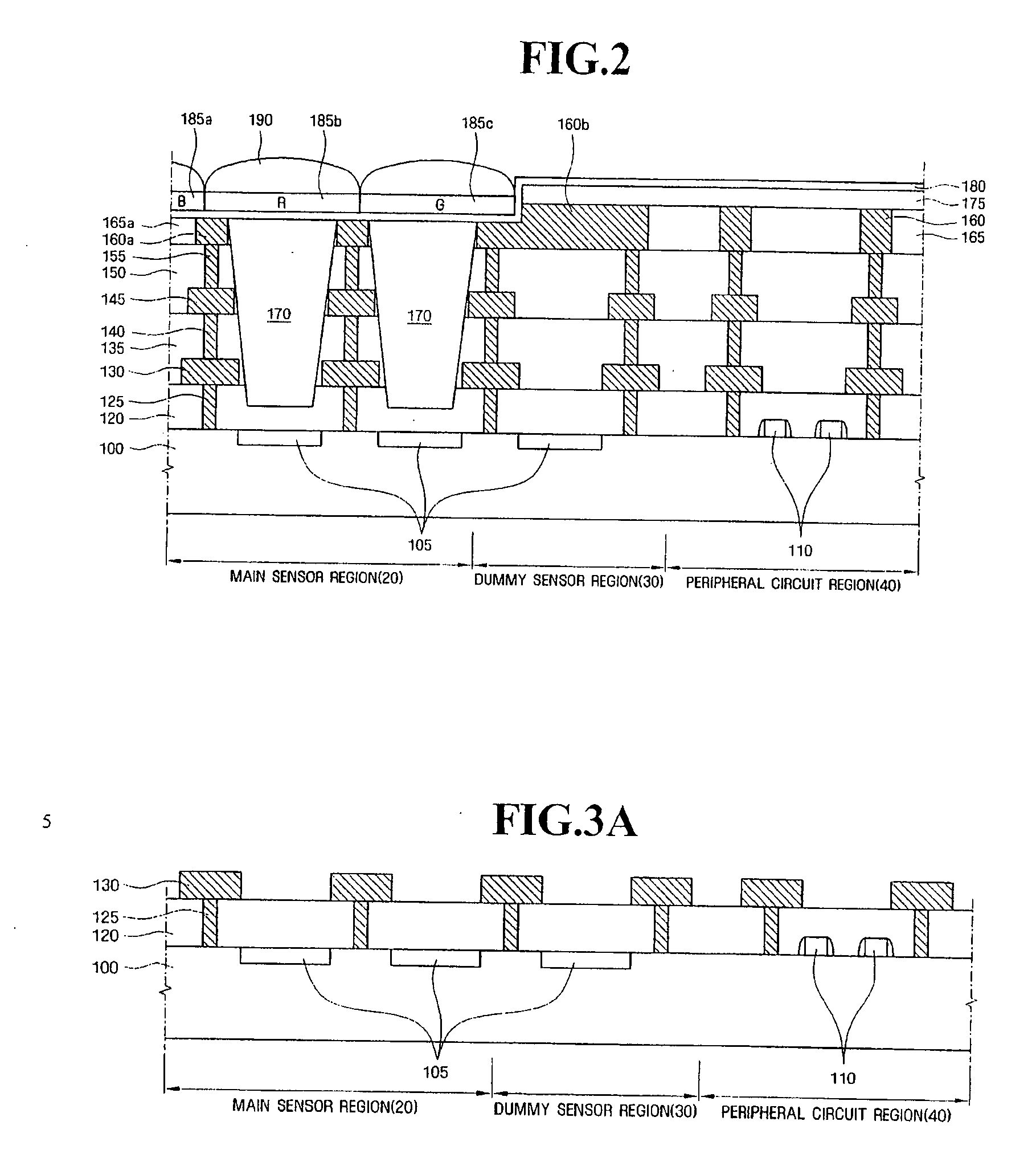
[0039]Reference now should be made to the drawings, in which the same reference numerals are used throughout the different drawings to designate the same or similar components. Embodiments of the present invention are described in detail below with reference to the accompanying drawings.

[0040]It will be understood that when an element is referred to as being “on” or “connected” or “coupled” to another element, it can be directly on or connected or coupled to the other element or intervening elements can be present. In contrast, when an element is referred to as being “directly on” or “directly connected” or “directly coupled” to another element, there are no intervening elements present. Other words used to describe the relationship between elements should be interpreted in a like fashion (e.g., “between” versus “directly between,”“adjacent” versus “directly adjacent,” etc.).

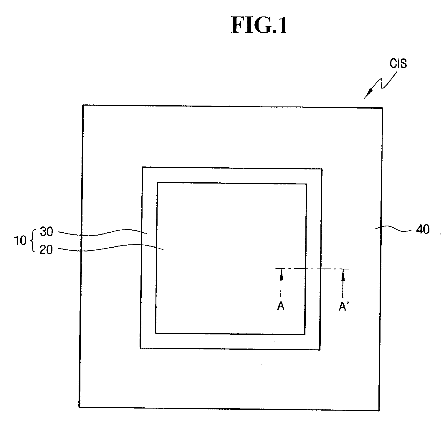
[0041]FIG. 1 is a plan view illustrating a image sensor CIS according to an embodiment of the present inventi...


PUM


Abstract

In an image sensor in which a vertical length from a photoelectric conversion element to an uppermost micro-lens is minimal, and a method of manufacturing the same, the image sensor includes a substrate, a plurality of photoelectric conversion elements, and first to n-level (where n is an integer greater than or equal to 2) metal wires. In the substrate, a sensor region and a peripheral circuit region are defined. The plurality of photoelectric conversion elements are formed in or on the substrate within the sensor region. The first to n-level metal wires are sequentially formed on the substrate. The n-level metal wires within the sensor region are of a thickness that is less than the n-level metal wires within the peripheral circuit region.

Description

CROSS-REFERENCE TO RELATED APPLICATION[0001]This application is based on and claims priority to Korean Patent Application No. 10-2006-0076334 filed on Aug. 11, 2006 in the Korean Intellectual Property Office, the disclosure of which is incorporated herein in its entirety by reference.BACKGROUND OF THE INVENTION[0002]1. Field of the Invention[0003]The present invention relates generally to an image sensor and a method of manufacturing the same, and more particularly to a CMOS image sensor and a method of manufacturing the same.[0004]2. Description of the Related Art[0005]An image sensor converts an optical image to electrical signals. With the continued development of the computer and communication industries, the demand for image sensors has rapidly increased as devices including digital cameras, camcorders, security cameras, and micro-cameras for medical purposes employ image sensors.[0006]A CMOS image sensor offers operation ease, and can be implemented using various scanning meth...

Claims


Application Information

Patent Timeline
IPC IPC(8): H01L31/0232H01L31/18
CPCH01L27/14621H01L27/14625H01L27/14685H01L27/14636H01L27/14627H01L27/146
Inventor PARK, BYUNG-JUN
Owner SAMSUNG ELECTRONICS CO LTD
Why Eureka
Try Eureka