

Photoelectric conversion element and interconnector-equipped photoelectric conversion element
a technology of photoelectric conversion element and interconnector, which is applied in the direction of photovoltaics, electrical devices, semiconductor devices, etc., can solve the problems of photoelectric conversion layer damage photoelectric conversion layer cracks, etc., and achieve the effect of reducing the occurrence of cracks in the photoelectric conversion layer
- Summary
- Abstract
- Description
- Claims
- Application Information
AI Technical Summary
Benefits of technology
Problems solved by technology
Method used
Image

Examples
example
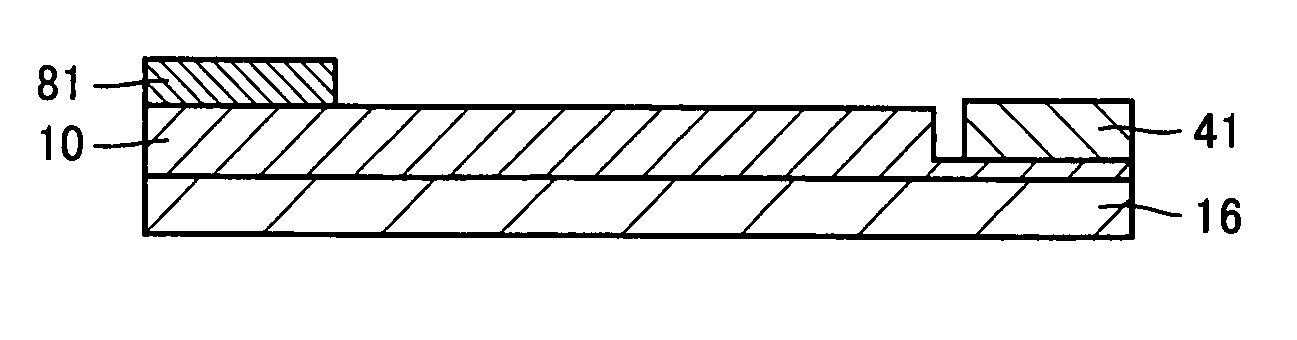
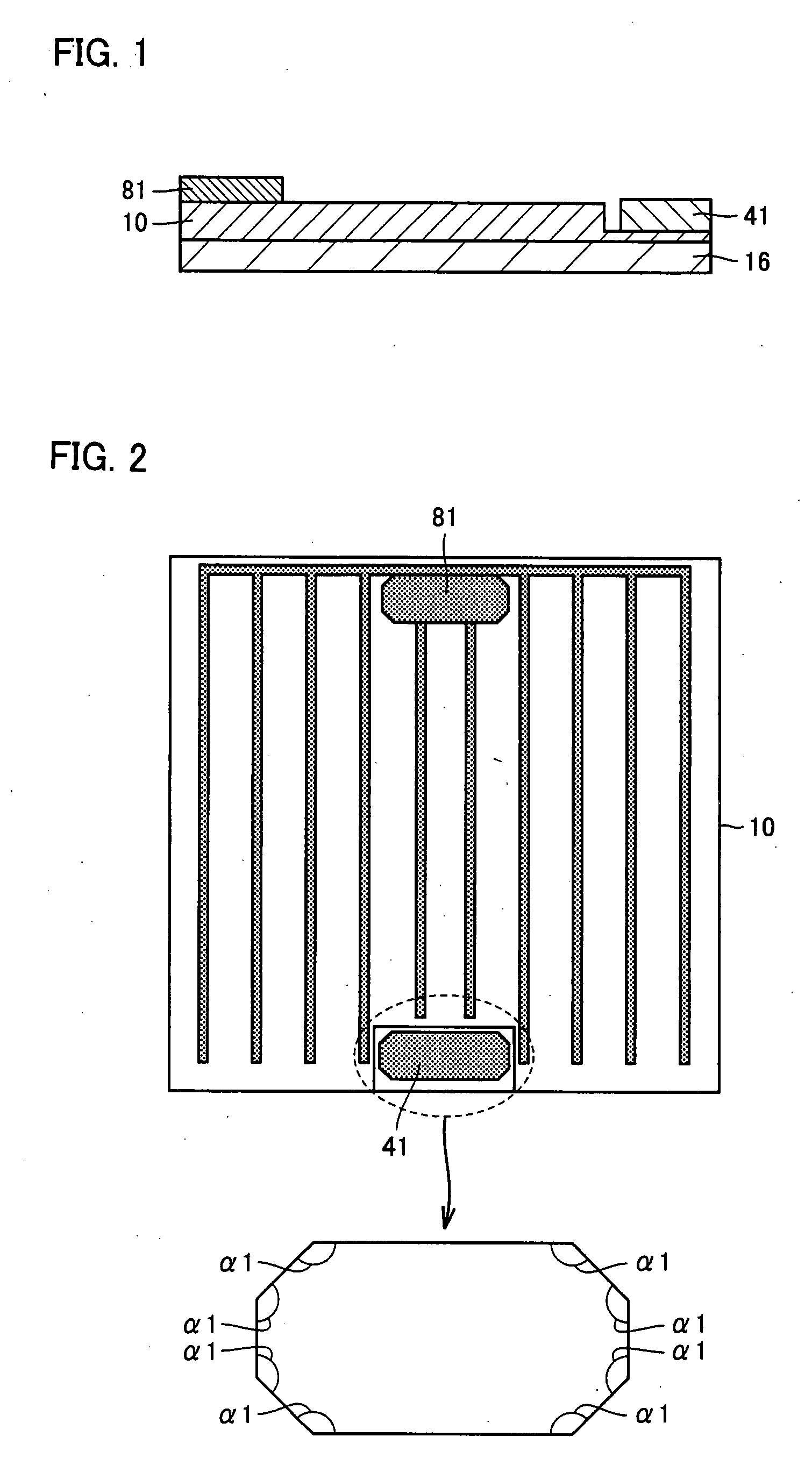
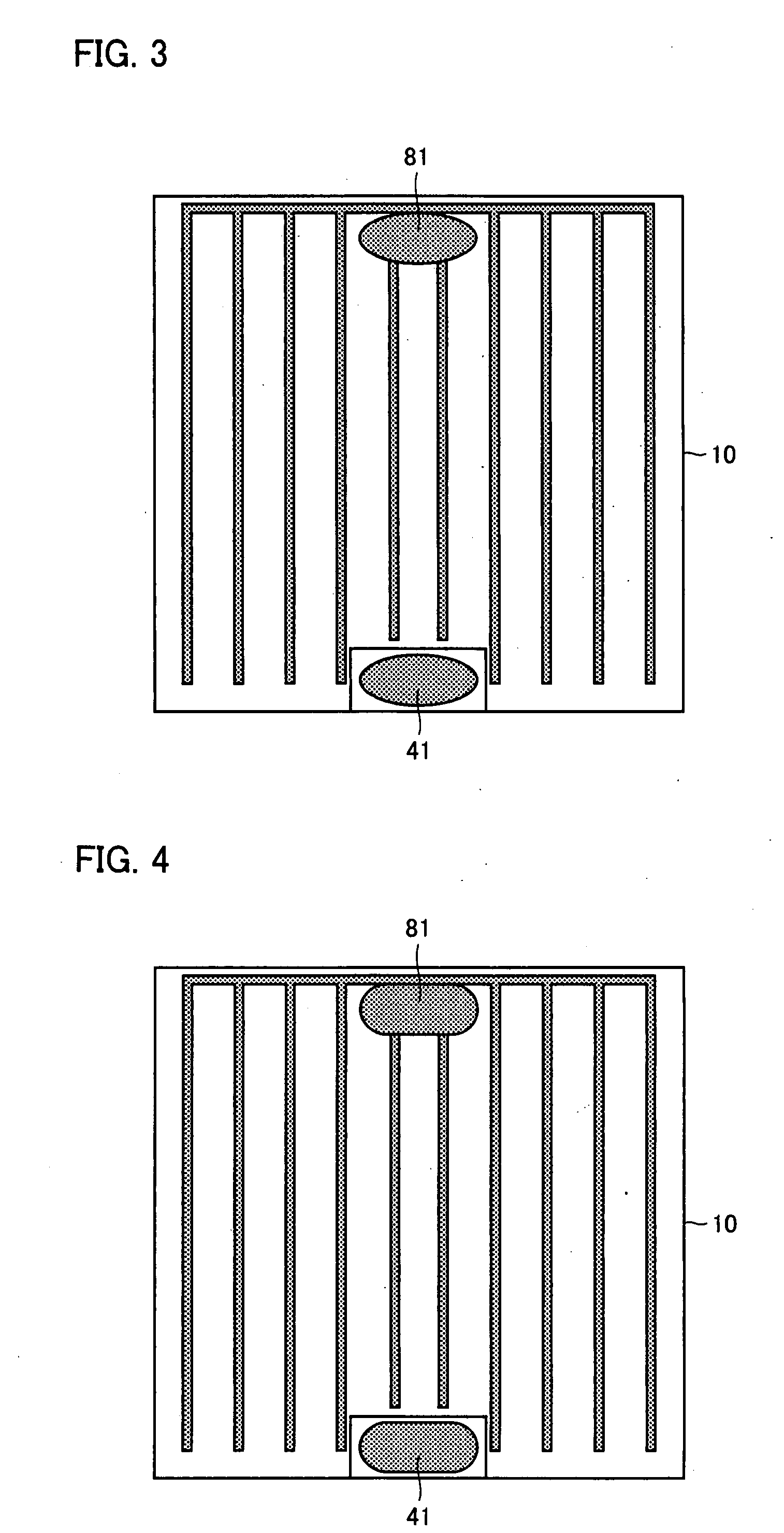
[0070]Firstly, an n-type GaAs layer was formed on a p-type Ge substrate doped with Ga. On that occasion, As in the n-type GaAs layer was diffused into the p-type Ge substrate, and thus an n-type Ge layer was formed on a surface of the p-type Ge substrate. Next, an n-type InGaP layer, a p-type AlGaAs layer, a p-type InGaP layer, a p-type GaAs layer, an n-type GaAs layer, an n-type AlInP layer, an n-type InGaP layer, a p-type AlGaAs layer, a p-type AlInP layer, a p-type InGaP layer, an n-type InGaP layer, an n-type AlInP layer, and an n-type GaAs layer were epitaxially grown in this order on the n-type GaAs layer, and thus a photoelectric conversion layer having at least one pn junction was formed on the p-type Ge substrate. The photoelectric conversion layer had an overall thickness of 4 μm.
[0071]Then, an Au—Ge film, a Ni film, an Au film, and an Ag film were deposited in this order on a surface of the n-type GaAs layer, which was the uppermost surface of the photoelectric conversion...
PUM
 Abstract
Description
Claims
Application Information