Display device

a display device and anti-reflection film technology, applied in the field of display devices, can solve the problems of difficult anti-reflection treatment of all external light beams, limited functionality of conventional anti-reflection film, etc., and achieve the effect of reducing the amount of external light reflected to the viewer side, increasing the number of times of external light entering the display device on the anti-reflection film, and increasing the amount of external light transmitted through the anti-reflection film

Inactive Publication Date: 2008-02-21
SEMICON ENERGY LAB CO LTD
View PDF43 Cites 66 Cited by
  • Summary
  • Abstract
  • Description
  • Claims
  • Application Information

AI Technical Summary

Benefits of technology

[0020] In other words, the number of times of incidence of external light entering the display device on the anti-reflection film is increased; therefore, the amount of external light transmitted through the anti-reflection film is increased. Thus, the amount of external light reflected to a viewer side is reduced, and the cause of a reduction in visibility such as reflection can be eliminated.
[0021] Furthermore, since the protective layer is formed between the projections in the present invention, the entry of a contaminant such as dust into between the projections can be prevented. Therefore, a decrease of an anti-ref

Problems solved by technology

However, with the above-described multilayer structure, a light beam, which cannot be cancelled, of the external light beams reflected at each layer interface is emitted to a viewer side as reflected light.
In order to achieve mutual cancellation of external light beams, it is necessary to precisely control optical characteristics of materials, thicknesses, and the like of films

Method used


Image

  • Display device
  • Display device
  • Display device

Examples


embodiment mode 1

[0061] This embodiment mode describes an example of a display device having an anti-reflection function that can further reduce reflection of external light, for the purpose of providing excellent visibility.

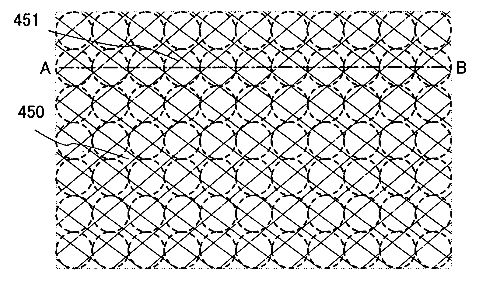
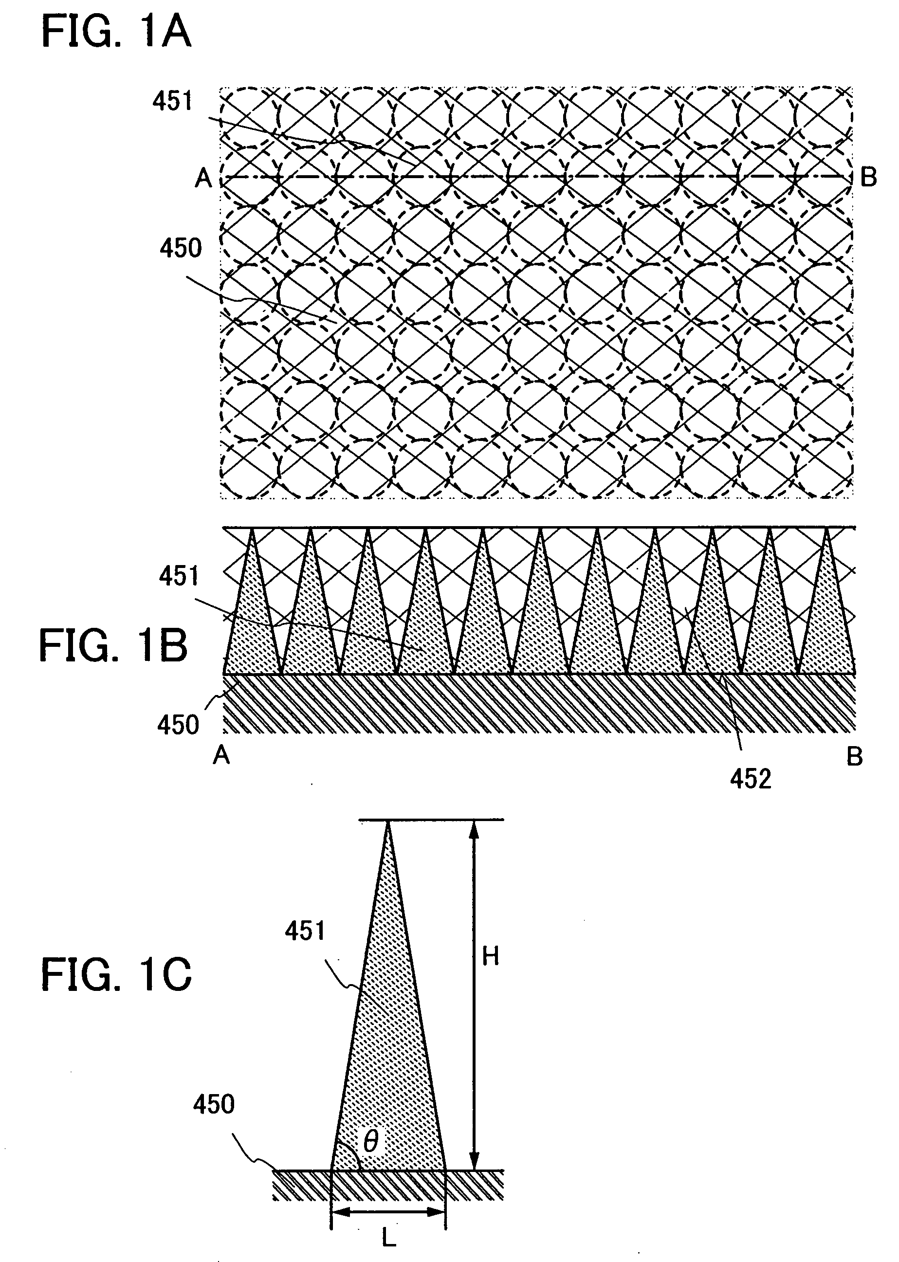
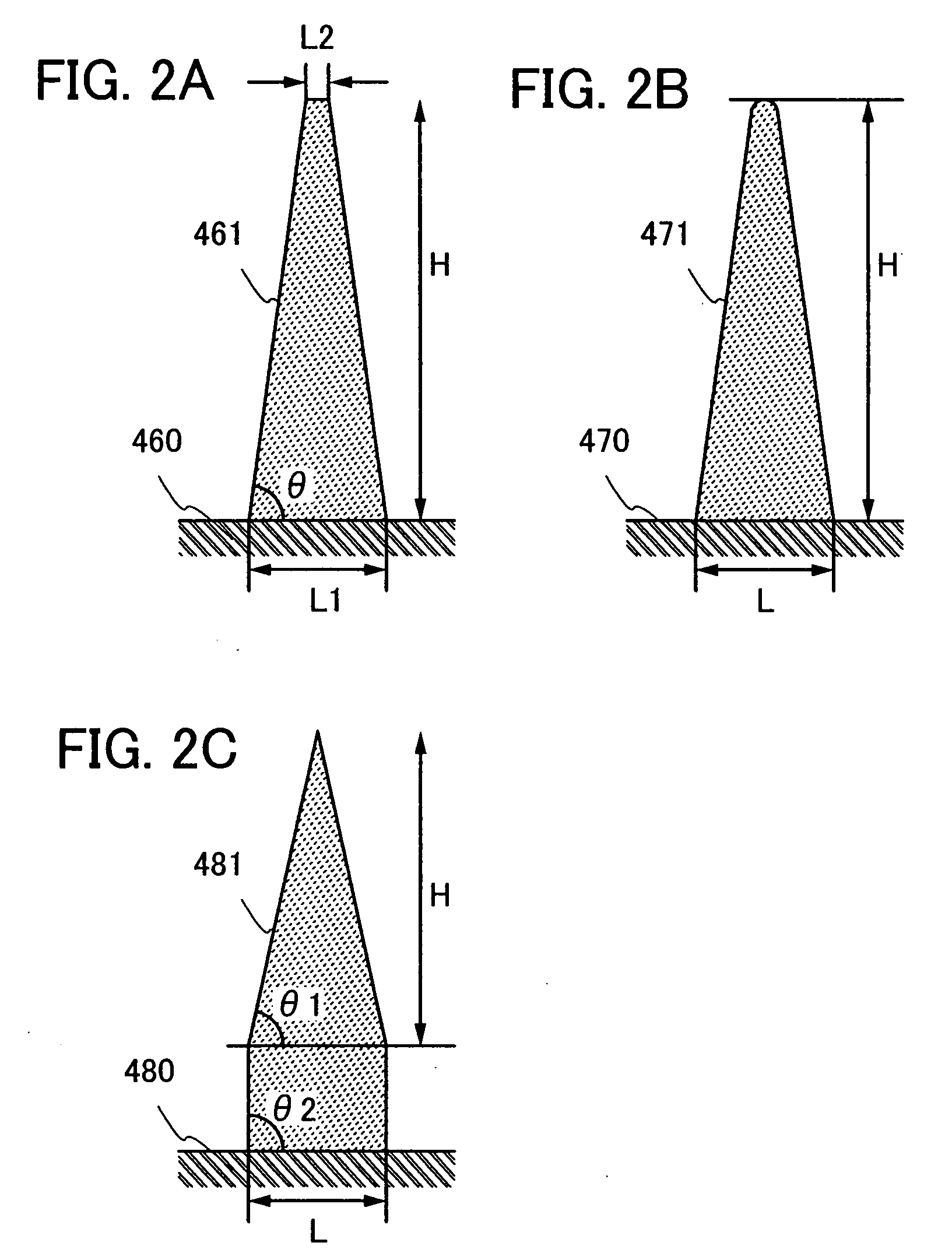
[0062] A feature of the present invention is to use an anti-reflection film having a plurality of projections over a display screen surface of a display device as an anti-reflection film having an anti-reflection function that prevents reflection of external light. Each projection of the anti-reflection film of the present invention preferably has a conical shape, and an angle made by a base and a lateral surface of each projection is preferably equal to or greater than 84° and less than 90°.

[0063]FIG. 1A shows a top view and FIGS. 1B and 1C show cross-sectional views of the anti-reflection film of the present invention. In FIGS. 1A to 1C, a plurality of projections 451 and a protective layer 452 are provided over a display screen surface of a display device 450. FIG. 1A is a ...

embodiment mode 2

[0091] This embodiment mode describes an example of a display device having an anti-reflection function that can further reduce reflection of external light, for the purpose of providing excellent visibility. Specifically, this embodiment mode describes a case of a display device having a passive-matrix structure.

[0092] The display device includes a first electrode layer 751a, a first electrode layer 751b, and a first electrode layer 751c which extend in a first direction; an electroluminescent layer 752 which is provided to cover the first electrode layer 751a, the first electrode layer 751b, and the first electrode layer 751c; and a second electrode layer 753a, a second electrode layer 753b, and a second electrode layer 753c which extend in a second direction perpendicular to the first direction (see FIGS. 5A and 5B). The electroluminescent layer 752 is provided between the first electrode layer 751a, the first electrode layer 751b, and the first electrode layer 751c and the seco...

embodiment mode 3

)

[0111] This embodiment mode describes an example of a display device having an anti-reflection function that can further reduce reflection of external light, for the purpose of providing excellent visibility. This embodiment mode describes a display device having a different structure from that of Embodiment Mode 2. Specifically, this embodiment mode describes a case where the display device has an active-matrix structure.

[0112]FIG. 36A shows a top view of the display device, and FIG. 36B shows a cross-sectional view of FIG. 36A taken along a line E-F. Although an electroluminescent layer 532, a second electrode layer 533, and an insulating layer 534 are omitted and not shown in FIG. 36A, each of them is provided as shown in FIG. 36B.

[0113] First wirings that extend in a first direction and second wirings that extend in a second direction perpendicular to the first direction are provided over a substrate 520 provided with an insulating layer 523 as a base film. One of the first w...


PUM

PropertyMeasurementUnit
Angleaaaaaaaaaa
Angleaaaaaaaaaa
Diameteraaaaaaaaaa

Abstract

The display device includes an anti-reflection film having a plurality of projections over a display screen surface and a protective layer filling a space between the projections. The number of times of incidence of external light entering the display device on the anti-reflection film is increased; therefore, the amount of external light transmitted through the anti-reflection film is increased. Thus, the amount of external light reflected to a viewer side is reduced, and the cause of a reduction in visibility such as reflection can be eliminated. Further, since the plurality of projections is covered with a protective layer, entry of dust can be prevented, and physical strength of the anti-reflection film can be increased.

Description

TECHNICAL FIELD [0001] The present invention relates to a display device having an anti-reflection function. BACKGROUND ART [0002] In some display devices having various displays (such as a liquid crystal display, an electroluminescent display (hereinafter also referred to as an EL display), or a plasma display), there may be a case where it becomes difficult to see a display screen due to reflection of its surroundings by surface reflection of external light, so that visibility is decreased. This is a considerable problem particularly in an increase in size of the display device and outdoor use thereof. [0003] In order to prevent such reflection of external light, a method of providing a display screen of a display device with an anti-reflection film has been employed. For example, there is a method of providing an anti-reflective film that has a multilayer structure of stacked layers having different refractive indices so as to be widely effective for a visible light wavelength ra...

Claims


Application Information

Patent Timeline
IPC IPC(8): G09G3/34G09F9/00G02B1/11G02B1/113G02F1/1335G02F1/136G09F9/30H01L27/32H01L51/50H05B33/02H05B33/14
CPCC09K11/06C09K2211/1011C09K2211/1029C09K2211/185G02B1/118Y10T428/10H01J2211/442H01L27/3244H01L51/5281H05B33/22G02F1/133502C09K2323/00H10K59/12H10K50/86G02B1/111G02B5/3033G02B1/14
Inventor EGI, YUJINISHI, TAKESHIOGINO, KIYOFUMISASAGAWA, SHINYAKURATA, MOTOMUSUZAWA, HIDEOMI
Owner SEMICON ENERGY LAB CO LTD
Why Eureka
Try Eureka