

Display Device
- Summary
- Abstract
- Description
- Claims
- Application Information
AI Technical Summary
Benefits of technology
Problems solved by technology
Method used
Image

Examples
specific embodiment
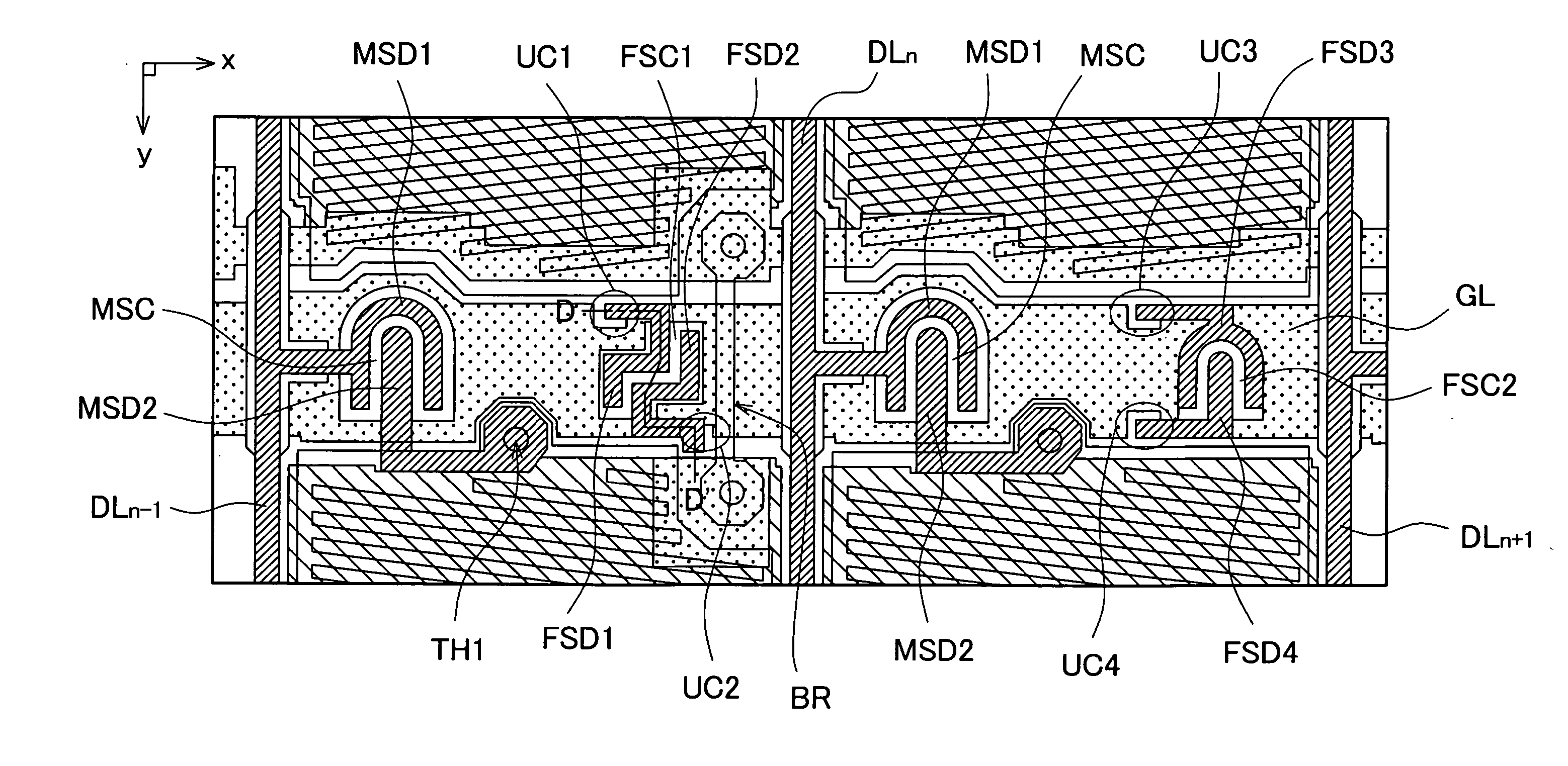
[0064]FIG. 6 and FIG. 7 are schematic views showing the schematic constitution of the TFT substrate of one specific embodiment according to the present invention.
[0065]FIG. 6 is a schematic plan view showing a constitutional example of a TFT element of the TFT substrate of this embodiment. FIG. 7 is a schematic cross-sectional view taken along a line D-D′ in FIG. 6.
[0066] The TFT substrate 1 of this embodiment is a TFT substrate which is used in a liquid crystal display panel of a lateral-electric-field driving method in which one pixel is configured as shown in FIG. 3 to FIG. 5. Further, in the TFT substrate of this embodiment, in one pixel region which is surrounded by two neighboring scanning signal lines and two neighboring video signal lines, a first TFT element which is used in an initial state and a second TFT element (spare TFT element) which is used when a malfunction occurs in the first TFT element are arranged.
[0067] Further, in the TFT substrate 1 shown in FIG. 3 to F...
PUM
 Abstract
Description
Claims
Application Information