Trilayer resist scheme for gate etching applications

a gate etching and resist scheme technology, applied in the field of integrated circuits, can solve the problems of significant resist loss and minimal resist budget for transferring a pattern through a 100 nm polysi gate conductor, and achieve the effect of minimizing the extend of ler and lwr, and avoiding flopping or buckling

Inactive Publication Date: 2008-02-21
GLOBALFOUNDRIES INC
View PDF4 Cites 15 Cited by
  • Summary
  • Abstract
  • Description
  • Claims
  • Application Information

AI Technical Summary

Benefits of technology

[0010]Since the thickness of the bottom organic layer of the inventive TLR can be arbitrarily chosen to meet resist budget requirements, sufficient budget exists for completing the etch process and minimizing the extend of LER and LWR that typically occurs with diminished resist budgets. Further, since the degree / extent of over etching during the etching of the bottom organic layer determines the final gate CD, this can be tailored to a desired value (less than 40 nm), the minimum value of which is now limited by the aspect ratio of the bottom organic layer and the mechanical integrity of this layer itself.
[0011]For pre-doped nFET devices, the pre-doped gate conductor layer isotropically etches in fluorine, chlorine or HBr chemistries. As such, passivation of the sidewall of the pre-doped layer during the gate conductor etch process becomes significant for maintaining an ideal gate profile. This necessary condition sets up a trade-off between the former (passivation of the pre-doped layer) and maintaining the profile of the bottom organic layer. The process window for this tradeoff can be carefully widened by choosing the appropriate thickness of the bottom organic layer such that the aspect ratio of this layer enables a sufficiently wide process window for pre-doped gate conductor passivation and an ideal profile of this masking layer (i.e., avoiding flop over or buckling). In this manner, gate CDs of about 25 nm are feasible at 0.1 μm2 ground rules.

Problems solved by technology

In the prior art, the resist thicknesses for 65 nm and beyond technologies are less than or equal to 200 nm, further, given lithographic limitations it is necessary to perform an isotropic etch (i.e., trimming step) of the resist so as to achieve the target CD, both this and the etching of the ARC results in significant resist loss and minimal resist budget for transferring a pattern through a 100 nm polySi gate conductor.

Method used


Image

  • Trilayer resist scheme for gate etching applications
  • Trilayer resist scheme for gate etching applications
  • Trilayer resist scheme for gate etching applications

Examples


Embodiment Construction

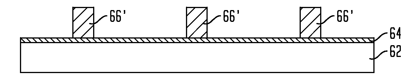
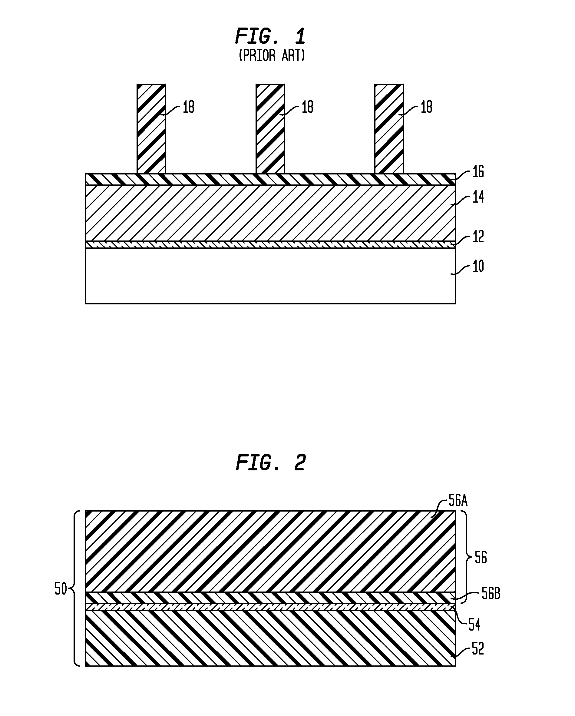
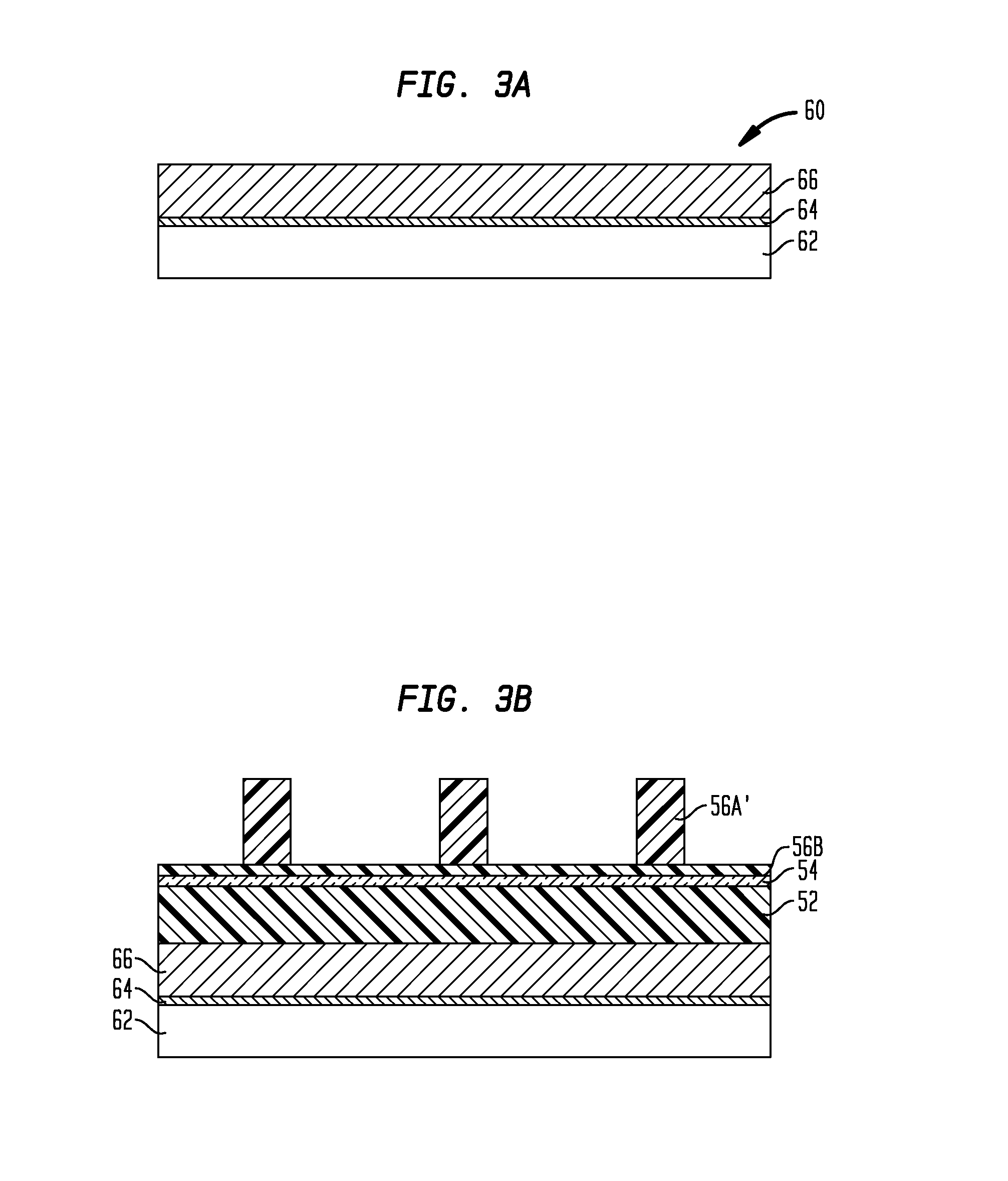
[0032]The present invention, which provides a trilayer resist (TLR) scheme for gate etching applications and CMOS structures formed by utilizing the same, will now be described in greater detail by referring to the following discussion and drawings that accompany the present application. It is noted that the drawings including the cross sectional views are provided for illustrative purposes and, as such, the same are not drawn to scale.

[0033]In the following description, numerous specific details are set forth, such as particular structures, components, materials, dimensions, processing steps and techniques, in order to provide a thorough understanding of the present invention. However, it will be appreciated by one of ordinary skill in the art that the invention may be practiced without these specific details. In other instances, well-known structures or processing steps have not been described in detail in order to avoid obscuring the invention.

[0034]It will be understood that whe...


PUM


Abstract

A trilayer resist (TLR) patterning scheme is provided to enable gate conductors, particularly polySi gate conductors, with critical dimensions (CDs) of less than 40 nm and minimal LER and LWR. In accordance with the present invention, the inventive patterning scheme utilizes an organic/inorganic/organic multilayer stack instead of an organic layer used in the prior art. The top organic layer of the inventive TLR is a photoresist material such as a 193 nm photoresist that is located atop an antireflective coating (ARC), which is also comprised of an organic material. The middle inorganic layer of the TLR comprises any oxide layer such as, for example, a low temperature (less than or equal to 250° C.) chemical vapor deposited (CVD) oxide, an oxide derived from TEOS (tetraethylorthosilicate), silicon oxide, a silane oxide, or a Si-containing ARC material. The bottom organic layer of the TLR comprises any organic layer such as, for example, a Near Frictionless Carbon (NFC), a diamond-like carbon, a thermosetting polyarylene ether.

Description

FIELD OF THE INVENTION[0001]The present invention generally relates to integrated circuits (ICs), and more particularly, to complementary metal oxide semiconductor (CMOS) devices such as, for example, n-type and / or p-type field effect transistors (FETs), in which an integration scheme is employed for achieving sub ground rule (on the order of less than 40 nm) gate critical dimension (CD) for 45 nm and beyond front-end-of-the-line (FEOL) technologies. The inventive integration scheme also improves gate width modulation and, thus, achieves higher speed devices and ring oscillators.BACKGROUND OF THE INVENTION[0002]Generally, semiconductor devices include a plurality of circuits which form an integrated circuit (IC) including, for example, chips, thin film packages and printed circuit boards. ICs can be useful for computers and electronic equipment and can contain millions of transistors and other circuit elements that are fabricated on the same semiconductor wafer.[0003]For the device ...

Claims


Application Information

Patent Timeline
Patent Type & Authority Applications(United States)
IPC IPC(8): H01L21/44
CPCH01L21/0332H01L21/32139H01L21/28123
Inventor FULLER, NICHOLAS C.DALTON, TIMOTHY J.ZHANG, YING
Owner GLOBALFOUNDRIES INC
Why Eureka
Try Eureka