Signal analysis system and calibration method for measuring the impedance of a device under test

a technology of signal analysis and calibration method, which is applied in the field of signal analysis systems, can solve the problems of significant probe loading of the circuit under test, and the waveform received via the probe loading such a circuit may not accurately represent the voltage of the circui

Active Publication Date: 2008-02-28
TEKTRONIX INC
View PDF30 Cites 43 Cited by
  • Summary
  • Abstract
  • Description
  • Claims
  • Application Information

AI Technical Summary

Benefits of technology

[0008]The device under test may be a signal source and a passive circuit device coupled to the signal source. In such a configuration, sets of time domain samples of the signal under test are acquired from the signal source with selected impedance load inserted into the signal path. The sets of time domain samples are converted to frequency domain representations and transfer parameters of the signal source are characterized within a spectral domain from the spectral domain representations of the sets of samples. A reference impedance (Zref) associated with the signal analysis system is retrieved and processed with the transfer parameters of the signal source to effect thereby a representation of the signal source impedance (Zeqsource) as a function of frequency. The signal source is coupled to the passive circuit device. Sets of time domain samples of the signal under test are acquired from the passive circ

Problems solved by technology

This drop in impedance as frequency increases, coupled with the fact that many circuits being probed have a relatively low output impedance in the range of 25-150 ohms, results in a significant loading of

Method used


Image

  • Signal analysis system and calibration method for measuring the impedance of a device under test
  • Signal analysis system and calibration method for measuring the impedance of a device under test
  • Signal analysis system and calibration method for measuring the impedance of a device under test

Examples


Embodiment Construction

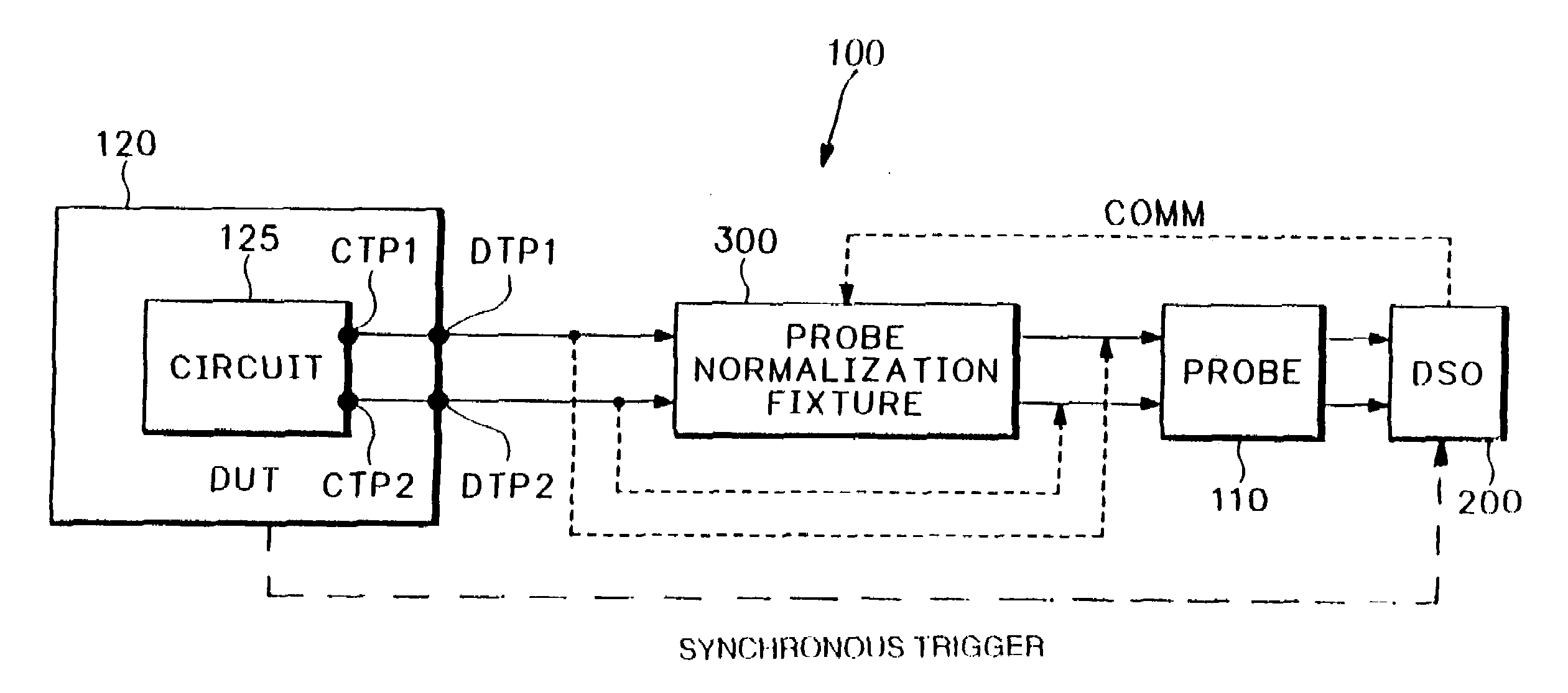
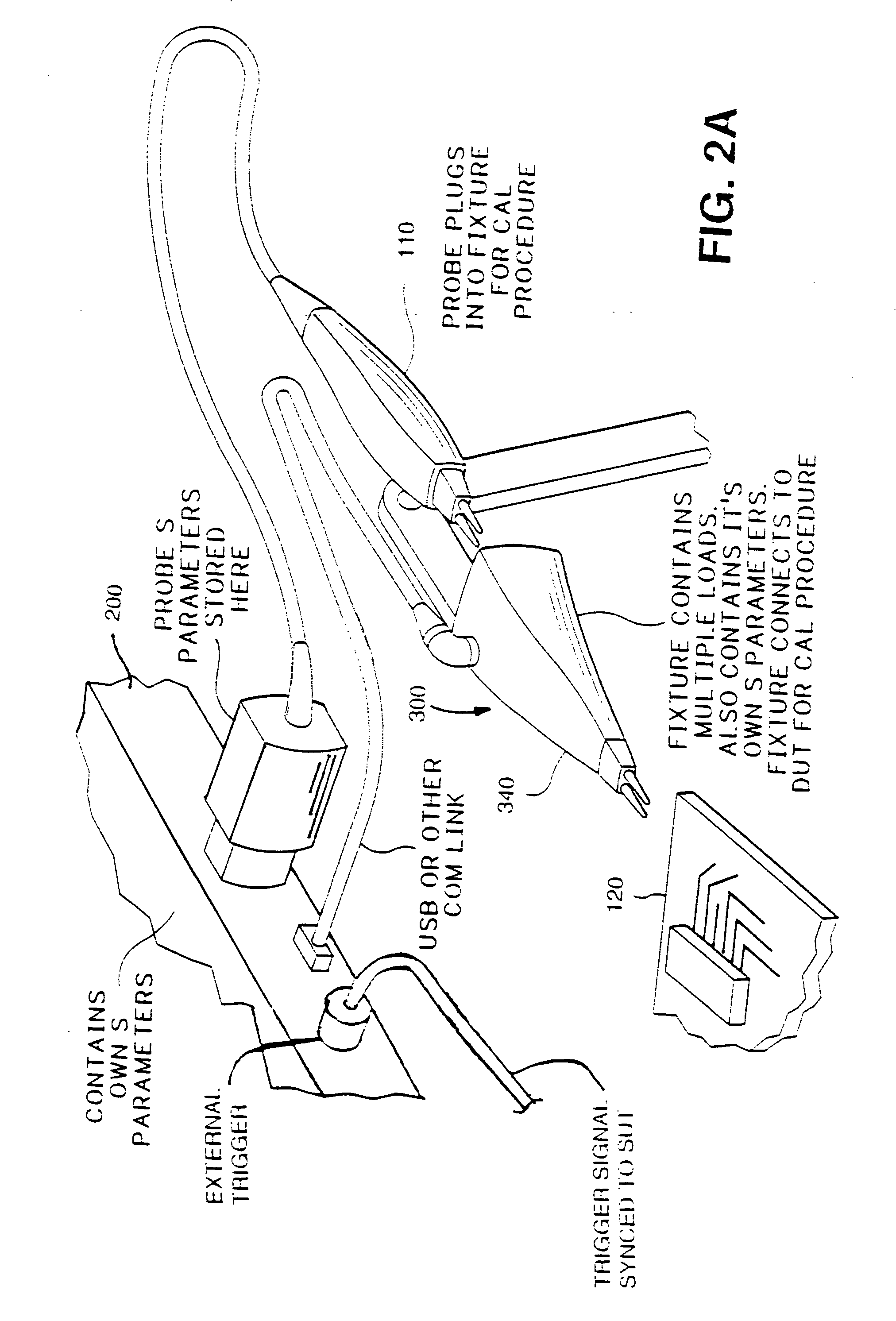
[0028]FIG. 1 depicts a high level block diagram of a signal analysis testing system 100 including a device under test arranged in accordance with various embodiments of the present invention. Specifically, a probe 110 is operably coupled to a signal analysis device such as a digital storage oscilloscope (DSO) 200 to provide thereto a signal under test (SUT) received from a device under test (DUT) 120. A probe normalization fixture 300 is selectively interposed between the DUT 120 and probe 110.

[0029]The invention operates to determine transfer parameters of a device under test in a signal path during the calibration of the signal path including the probe 110 and, optionally, DSO input channel. The calibration removes (i.e., de-embed) the signal degrading effects of elements in the signal path from the measurement of the DUT (or circuit) including transmission errors in the system. This de-embedding process is conducted by characterizing the probe 110 and other elements using a two-p...


PUM


Abstract

A method and apparatus adapted to calibrate a signal path of a signal analysis system such that digital samples of a signal under test acquired by the system are processed for representing the impedance of a device under test. The method and apparatus calibrates the signal path to characterize transfer parameters of the device under test within a spectral domain. A reference impedance (Zref) is retrieved that is associated with the signal analysis system. The transfer parameters of the device under test and the reference impedance (Zref) are processed to effect thereby a representation of the device under test impedance (Zeq) as a function of frequency.

Description

FIELD OF THE INVENTION[0001]The invention relates generally to signal analysis systems and, more particularly, to a system, apparatus and method for processing acquired digital samples of a test signal from device under test for producing an output representing an impedance of the device under test.BACKGROUND OF THE INVENTION[0002]Typical probes used for signal acquisition and analysis devices such as digital storage oscilloscopes (DSOs) and the like have an impedance associated with them which varies with frequency. For example, a typical probe may have an impedance of 100K to 200K Ohms at DC, which impedance drops towards 200 ohms at 1.5 GHz. Higher bandwidth probes drop to even lower impedance values. This drop in impedance as frequency increases, coupled with the fact that many circuits being probed have a relatively low output impedance in the range of 25-150 ohms, results in a significant loading of the circuit under test by the probe. As such, an acquired waveform received vi...

Claims


Application Information

Patent Timeline
IPC IPC(8): G01R27/04
CPCG01R35/005
Inventor TAN, KANPICKERD, JOHN J.QIU, PING
Owner TEKTRONIX INC
Why Eureka
Try Eureka