

Probe Card
a technology of probes and cards, applied in the field of probe cards, to achieve the effect of high-reliability inspection
- Summary
- Abstract
- Description
- Claims
- Application Information
AI Technical Summary
Benefits of technology
Problems solved by technology
Method used
Image

Examples
first embodiment
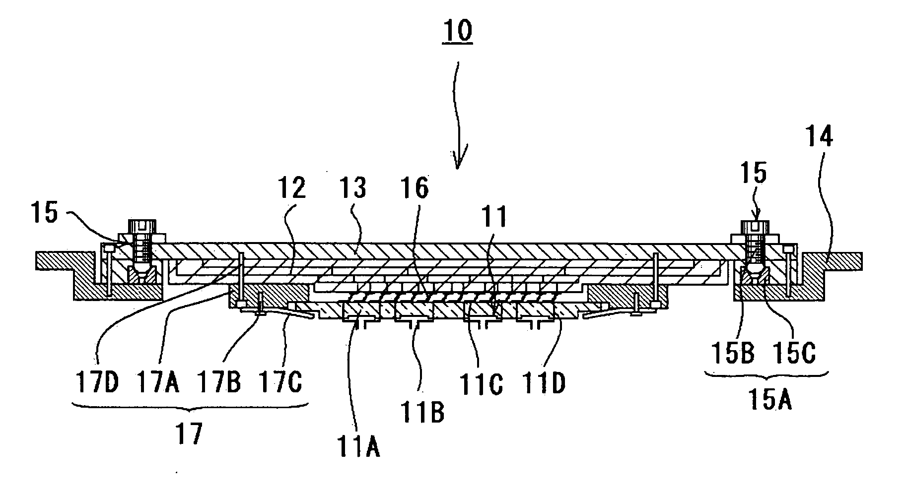
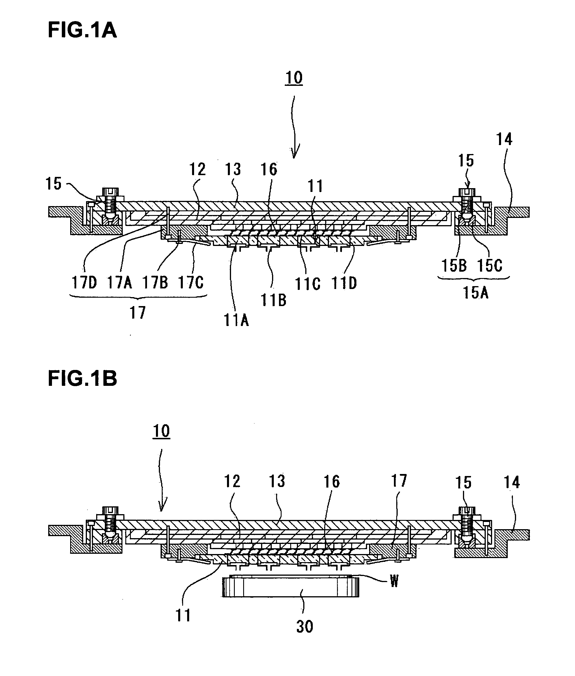
[0048] As shown in, for example, FIGS. 1(a), (b), a probe card 10 of this embodiment includes: a contactor 11; a printed wiring board 12 electrically connected to the contactor 11; and a reinforcing member 13 reinforcing the printed wiring board 12, and the probe card 10 is mounted in a prober (not shown) via a holder (card holder) 14 when in use. As shown in FIGS. 1(a), (b), in an outer peripheral edge portion of the probe card 10, provided is a parallelism adjustment mechanism 15 which adjusts a degree of parallelism between the contactor 11 and a wafer W disposed on a mounting table (main chuck) in the prober. The parallelism adjustment mechanism 15 has a plurality of parallelism adjustment means 15A which lift up the probe card 10 from the card holder 14.
[0049] Further, the contactor 11 and the printed wiring board 12 are electrically connected to each other via a plurality of contacts 16. These contacts 16 are made of conductive metal such as, for example, tungsten to be elast...
second embodiment
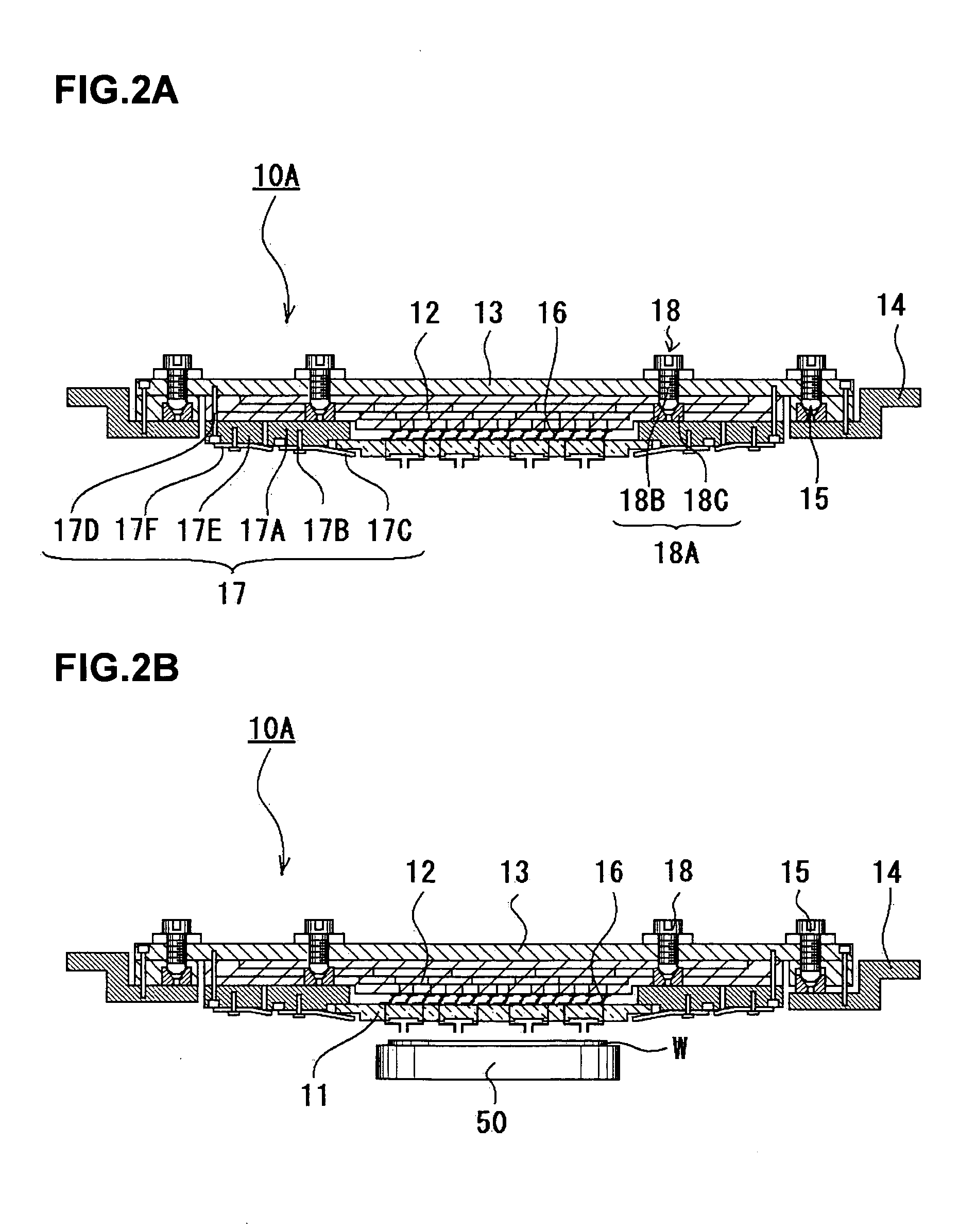
[0056] As shown in FIGS. 2(a), (b), a probe card 10A of this embodiment is structured in the same manner as the probe card 10 of the first embodiment except in that the probe card 10A has, in addition to the structure of the probe card 10 of the first embodiment, a pressure adjustment mechanism adjusting a pressure between a contactor and a printed wiring board. Therefore, in this embodiment, the same reference numerals and symbols are used to designate portions the same as or corresponding to those of the first embodiment, and characterizing portions of this embodiment will be mainly described.
[0057] As shown in FIGS. 2(a), (b), the probe card 10A of this embodiment includes: a parallelism adjustment mechanism 15; and a pressure adjustment mechanism 18 which is provided on an inner side of the parallelism adjustment mechanism 15 (concretely, for example, in a coupling portion) to adjust a contact pressure between a plurality of contacts 16 of a contactor 11 and a printed wiring bo...
third embodiment
[0062] A probe card 10B of this embodiment is structured in the same manner as the first embodiment except in that this embodiment uses, as an interposer, contacts having a substrate instead of the contacts 16 of the above-described embodiments, thereby improving contact failure due to thermal deformation of the probe card 10B. Therefore, in this embodiment, the same reference numerals and symbols are used to designate portions the same as or corresponding to those of the first embodiment, and characterizing portions of this embodiment will be mainly described.
[0063] For example, as shown in FIG. 3, the probe card 10B includes: a contactor 11; a printed wiring board 12; a coupling member 19 coupling and integrating the contactor 11 and the printed wiring board 12; and a reinforcing member 13 reinforcing the printed wiring board 12 integrated by the coupling member 19. Further, between the contactor 11 and the printed wiring board 12, an interposer 16 making the contactor 11 and the...
PUM
 Abstract
Description
Claims
Application Information