Active Matrix Substrate, Method for Correcting a Pixel Deffect Therein and Manufacturing Method Thereof

Active Publication Date: 2008-02-28
SHARP KK
View PDF6 Cites 32 Cited by
  • Summary
  • Abstract
  • Description
  • Claims
  • Application Information

AI Technical Summary

Benefits of technology

[0021] The present invention was made in view of the above mentioned problems and it is an object of the present invention to provide an active matrix substrate, a method of for correcting a pixel defect therein its and a manufacturing method, and a liquid crystal display device and its a manufacturing method, in which regarding a pixel defect caused by a short circuit between a

Problems solved by technology

In the manufacturing process of the active matrix substrate, a short circuit (leak) may generate between the source electrode and the drain electrode of the TFT, or the drain electrode or the drain extraction wiring is broken because of a foreign material, a film remaining and the like.
In addition, an operation defect of the TFT may generate because the ohmic contact is insufficiently provided.
Thus, a normal voltage (drain voltage) is not applied to the pixel electrode of the pixel in which the defect is generated, so that a point defect such as a luminance point or a black point is generated on a display screen in the liquid crystal display device, resulting in reduction of a manufacturing yield of the liquid crystal display device.
Therefore increase of an area of th

Method used


Image

  • Active Matrix Substrate, Method for Correcting a Pixel Deffect Therein and Manufacturing Method Thereof
  • Active Matrix Substrate, Method for Correcting a Pixel Deffect Therein and Manufacturing Method Thereof
  • Active Matrix Substrate, Method for Correcting a Pixel Deffect Therein and Manufacturing Method Thereof

Examples


embodiment 1

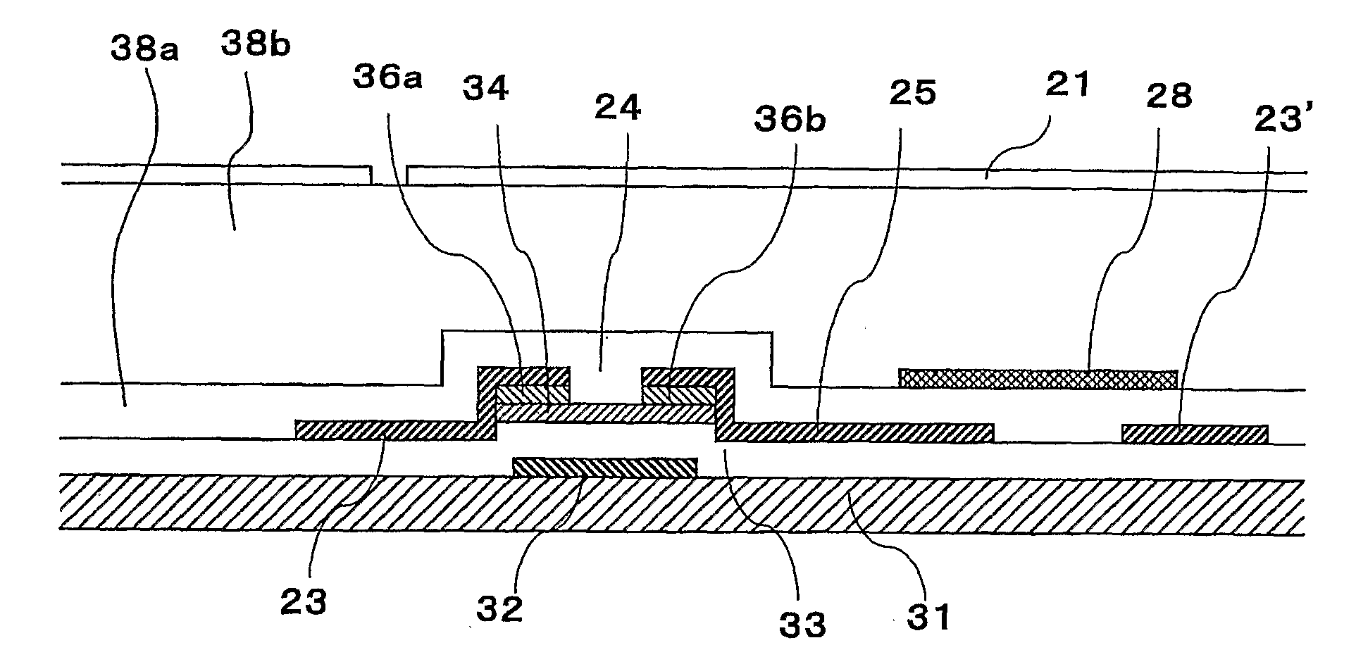
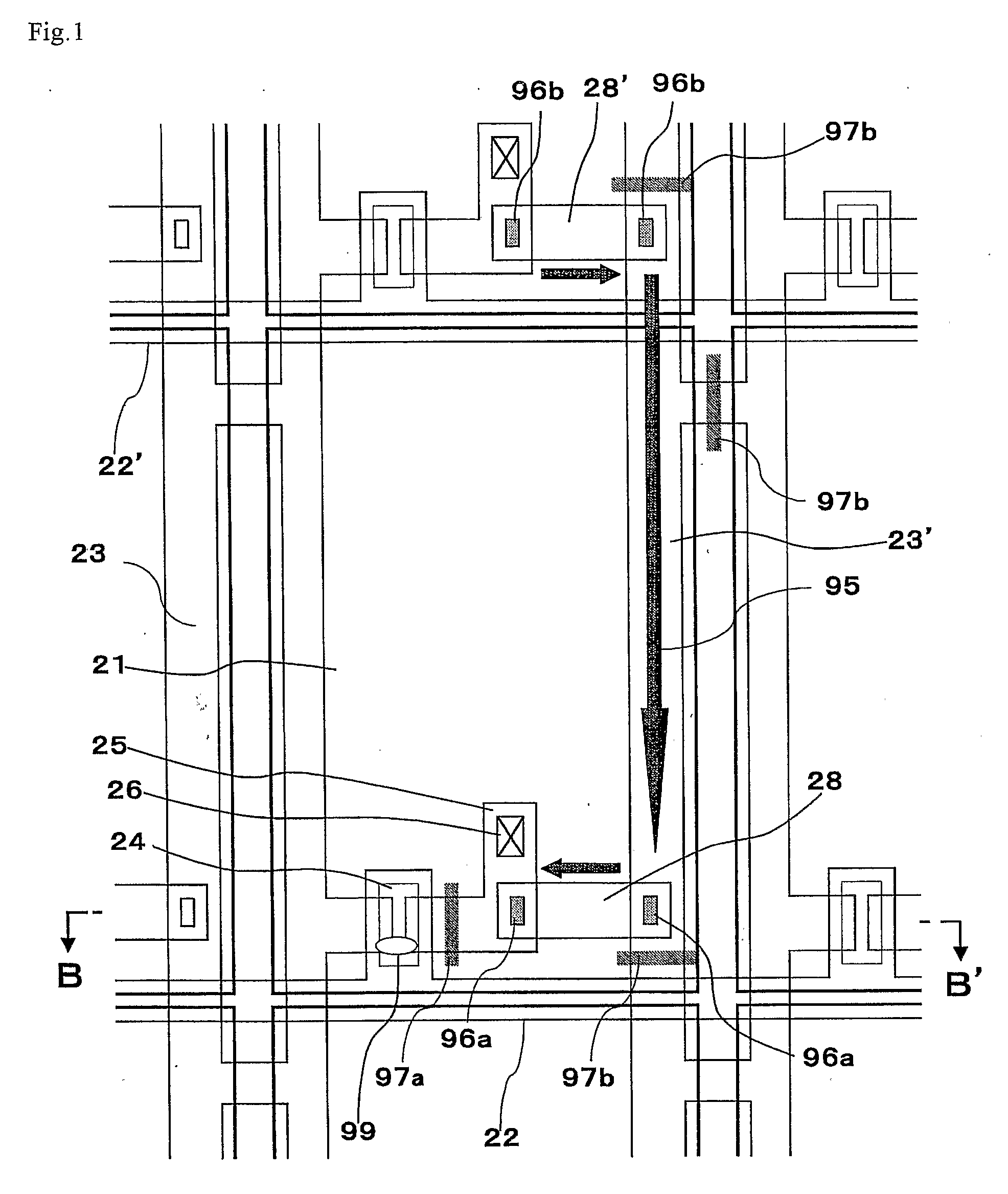
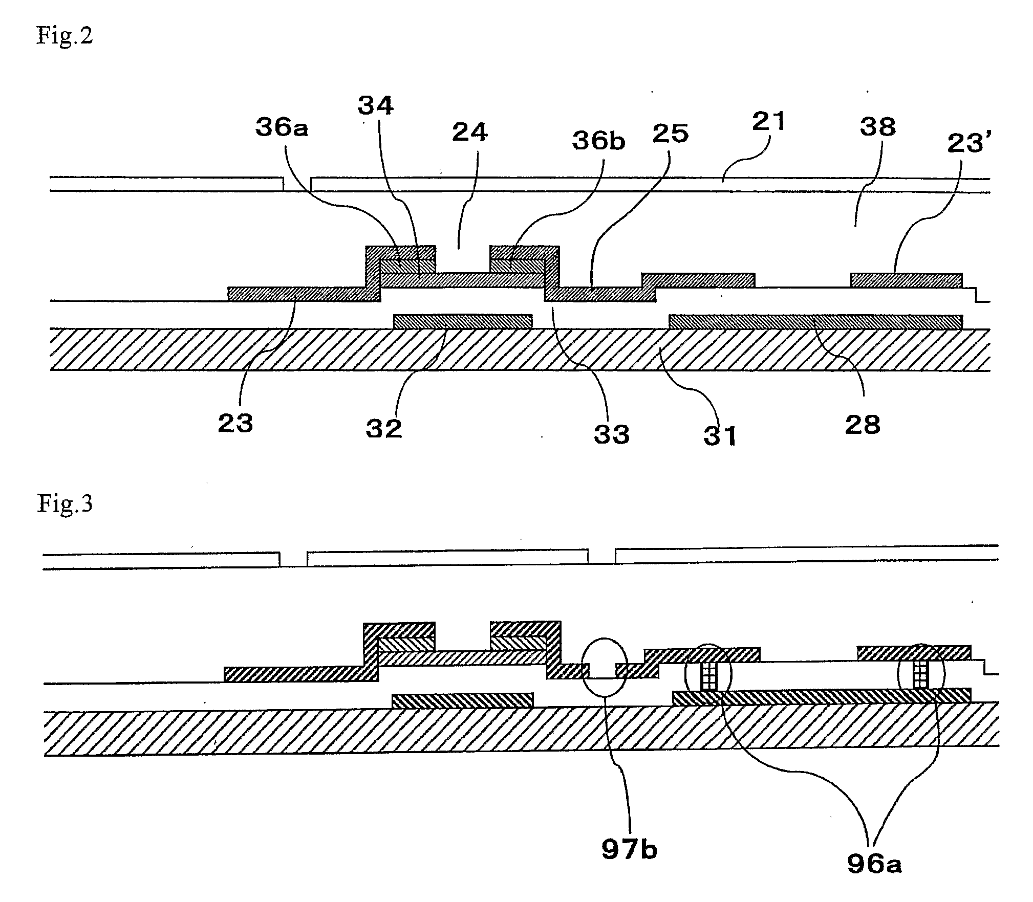
[0162] An embodiment 1 of the present invention will be described with reference to FIGS. 1 to 3. FIG. 1 is a schematic plan view showing a constitution of a pixel of an active matrix substrate according to the embodiment 1. As shown in FIG. 1, a plurality of the pixel electrodes 21 are provided on the active matrix substrate according to the embodiment 1 in the shape of a matrix. The scanning signal lines 22 and 22′ to supply a scanning line signal and the data signal lines 23 and 23′ to supply a data signal are provided so as to pass around the pixel electrodes 21 and intersect with each other. In addition, the data signal line 23′ is formed in the next stage (next column) of the data signal line 23 and the data signal lines 23 and 23′ are partly multilinear. The TFT 24 serving as a switching element to be connected to the pixel electrode 21 is provided at an intersecting part of the scanning signal lines 22 and 22′ with the data signal lines 23 and 23′. The scanning signal lines ...

embodiment 2

[0184] An embodiment 2 of the present invention will be described with reference to FIG. 7. FIG. 7 is a schematic plan view showing a constitution of a pixel of an active matrix substrate according to the embodiment 2. As shown in FIG. 7, a plurality of pixel electrodes 21 are provided on the active matrix substrate according to the embodiment 2 in a shape of a matrix. The scanning signal lines 22 and 22′ to supply a scanning signal and the data signal lines 23 and 23′ to supply a data signal are provided so as to pass around the pixel electrode 21 and intersect with each other. In addition, the data signal line 23′ is formed in the next stage (next column) of the data signal line 23 and the data signal lines 23 and 23′ are partly multilinear. The TFT 24 serving as a switching element to be connected to the pixel electrode 21 is provided at an intersecting part of the scanning signal lines 22 and 22′ with the data signal lines 23 and 23′. The scanning signal lines 22 and 22′ are con...

embodiment 3

[0193] An embodiment 3 of the present invention will be described with reference to FIG. 9. FIG. 9 is a schematic plan view showing a constitution of a pixel of an active matrix substrate according to the embodiment 3. As shown in FIG. 9, a plurality of pixel electrodes 21 are provided on the active matrix substrate according to the embodiment 3 in the shape of a matrix. The scanning signal lines 22 and 22′ to supply a scanning line signal and data signal lines 23 and 23′ to supply a data signal are provided so as to pass around the pixel electrode 21 and intersect with each other. In addition, the data signal line 23′ is formed in the next stage (next column) of the data signal line 23 and the data signal lines 23 and 23′ are partly multilinear. The TFT 24 serving as a switching element to be connected to the pixel electrode 21 is provided at an intersecting part of the scanning signal lines 22 and 22′ with the data signal lines 23 and 23′. The scanning signal lines 22 and 22′ are ...


PUM


Abstract

The present invention provides an active matrix substrate of comprising on the substrate: a plurality of scanning signal lines and data signal lines; a thin film transistor provided at an intersecting point of the signal lines and comprising a gate electrode connected to the scanning signal line, a source electrode connected to the data signal line; and a pixel electrode electrically connected to a drain electrode of the thin film transistor, wherein the active matrix substrate comprises a structure having an at least partly multilinear data signal line and an interconnection electrode for correction.

Description

BACKGROUND OF THE INVENTION [0001] 1. Field of the Invention [0002] The present invention relates to an active matrix substrate, pixel defect correcting method and its manufacturing method. More particularly, it relates to an active matrix substrate especially suitable for a component member of a liquid crystal display device having a pixel-divided (multi-pixel) structure, its pixel defect correcting method and manufacturing method, and a liquid crystal display device and its manufacturing method. [0003] 2. Background Art [0004] An active matrix substrates is widely used in active matrix display devices such as a liquid crystal display device, a EL (Electro Luminescence) display device and the like. According to the active matrix substrate used in a conventional active matrix display device, a switching element such as a TFT (Thin Film Transistor) and the like is provided at each intersecting point between a plurality of scanning signal lines and a plurality of data signal lines arr...

Claims


Application Information

Patent Timeline
IPC IPC(8): G02F1/1343G02F1/13H01J9/24G02F1/1362G02F1/1368G09F9/00G09F9/30H01L21/77H01L21/84H01L27/12H01L29/786
CPCG02F1/136213H01L27/124G02F2001/136268G02F1/136259G02F1/136268
Inventor YAGI, TOSHIFUMITAKEUCHI, MASANORITSUBATA, TOSHIHIDENAGASHIMA, NOBUYOSHIYAMAGUCHI, AKIRA
Owner SHARP KK
Why Eureka
Try Eureka