Method for producing semiconductor device

Inactive Publication Date: 2008-02-28
SONY CORP
View PDF33 Cites 27 Cited by
  • Summary
  • Abstract
  • Description
  • Claims
  • Application Information

AI Technical Summary

Benefits of technology

[0019]According to an embodiment of the present invention, the supporting substrate is bonded to the device layer including the devices, and the sacrificial layer is removed by etching to separate the device layer from the semiconductor substrate. The etching solution is allowed to penetrate to the entirety of the sacrificial layer through the grooves each extending from the device layer to the sacrificial layer. Thereby, the etching solution is surely allowed to penetrate from the middle portion to the periphery of the sacrificial layer, thus rapidly separating the device layer from the semiconductor substrate.
[0020]In this case, the grooves are in the form of a grid, each of the grooves being located between adjacent chips. Thereby, the etching solution is efficiently allowed to penetrate from the middle portion to the periphery of the sacrificial layer. Furthermore, the grooves are usable as dicing lines when the chips are formed.
[0021]With respect to the depth of each g

Problems solved by technology

However, the above-described method for producing a semiconductor device has disadvantages described below.
In the production of a device including expensive compound semiconductor, it takes a long time for etching a sacrificial layer by ELO.
From the view point, although Non-Pate

Method used


Image

  • Method for producing semiconductor device
  • Method for producing semiconductor device
  • Method for producing semiconductor device

Examples


Example

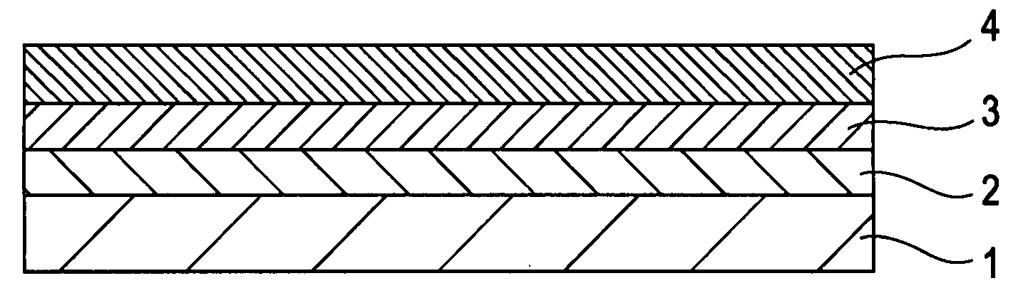
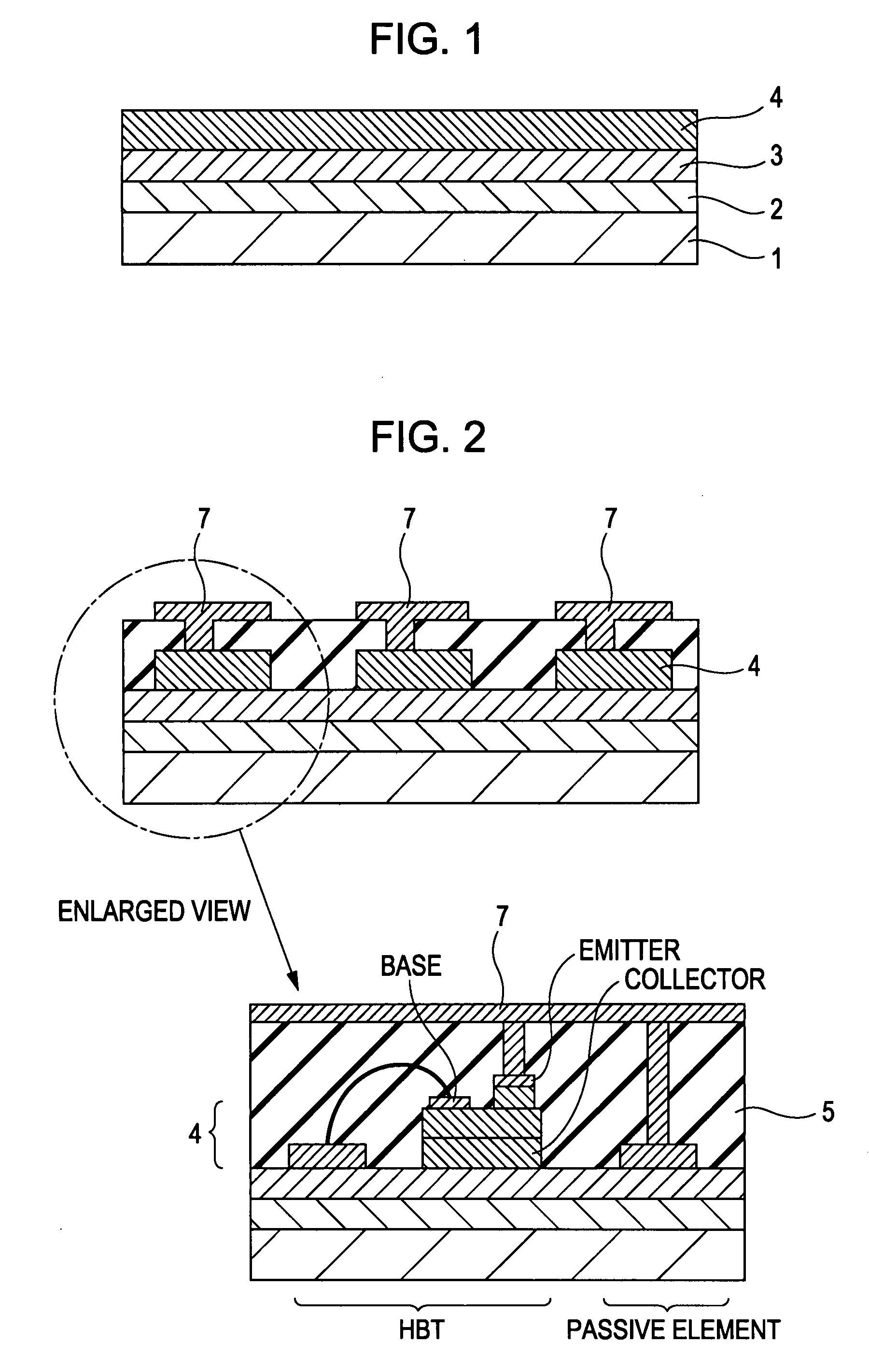
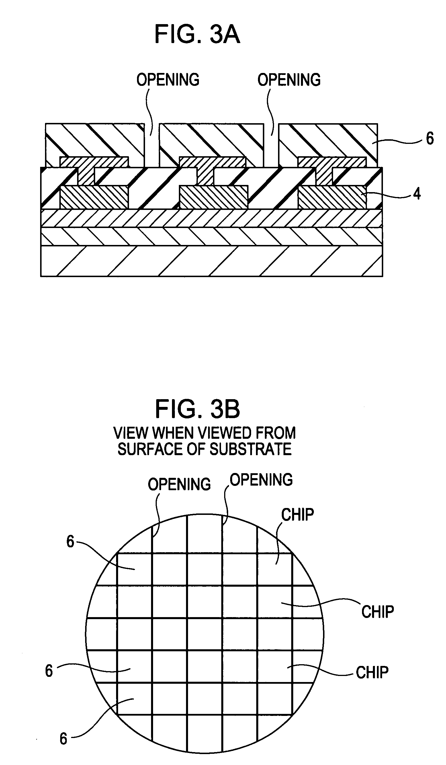
[0044]In a method according to an embodiment for producing a semiconductor device, monolithic microwave IC (MMIC) chips each including a high-In-content device produced by epitaxial lift-off (ELO) are exemplified. The method according to this embodiment for producing the MMIC chips has the following advantages.

1. A device layer is separated from a substrate by ELO to form MMIC chips.

[0045]2. Grooves which are in the form of a grid and which are each located between adjacent chips are formed in the device substrate side before the device substrate is bonded to a supporting substrate. The grooves in the form of a grid function as inlets for an etching solution that etches a sacrificial layer during the subsequent ELO step. In the ELO step, the penetration of the etching solution through the grooves results in the rapid completion of etching of the sacrificial layer.

3. The device layer is transferred to the supporting substrate while chip arrangement on the device substrate is maintain...


PUM


Abstract

A method for producing a semiconductor device includes the steps of forming a predetermined device in a device layer grown on a semiconductor substrate with a sacrificial layer provided therebetween; and removing the sacrificial layer by etching to separate the semiconductor substrate from the device layer while a supporting substrate is bonded to the side of the device layer, wherein in the step of removing the sacrificial layer, a groove extending from the device layer to the sacrificial layer is formed before the sacrificial layer is removed, and the etching solution is allowed to penetrate to the sacrificial layer through the groove.

Description

CROSS REFERENCES TO RELATED APPLICATIONS[0001]The present invention contains subject matter related to Japanese Patent Application JP 2006-224845 filed in the Japanese Patent Office on Aug. 22, 2006, the entire contents of which are incorporated herein by reference.BACKGROUND OF THE INVENTION[0002]1. Field of the Invention[0003]The present invention relates to a method for producing a semiconductor device by growing a device layer on a semiconductor substrate, forming a predetermined device in the device layer, and separating the device layer from the semiconductor substrate.[0004]2. Description of the Related Art[0005]Hitherto, the following devices including compound semiconductor materials and methods for producing the devices have been employed.High-In-Content Device[0006]Hetero-junction bipolar transistors (HBTs) each including InGaAs lattice-matched grown on an InP substrate and high-electron-mobility transistors (HEMTs) each including InGaAs / InAlAs have a balance between high...

Claims


Application Information

Patent Timeline
IPC IPC(8): H01L21/00
CPCH01L21/6835H01L21/78H01L2924/1305H01L2924/13064Y10S438/977H01L2924/014H01L2924/01072H01L2924/01023H01L2924/01006H01L2924/01005H01L2924/13063H01L2924/30105H01L2924/1517H01L2924/15153H01L2924/1423H01L2924/14H01L2924/10329H01L2924/09701H01L2924/01082H01L2924/01079H01L23/66H01L24/18H01L24/73H01L24/82H01L24/91H01L24/97H01L2221/68345H01L2224/18H01L2224/32225H01L2224/48091H01L2224/48227H01L2224/73265H01L2224/97H01L2924/01013H01L2924/01015H01L2924/01027H01L2924/01029H01L2924/01033H01L2924/01049H01L2924/01051H01L2924/01074H01L2924/01075H01L2924/00014H01L2924/00H01L2224/82H01L24/19H01L24/25H01L2224/04042H01L2224/04105H01L2224/2518H01L2224/73227H01L2224/73267H01L2924/3511
Inventor ONO, HIDEKITANIGUCHI, SATOSHI
Owner SONY CORP
Why Eureka
Try Eureka