Pop package and method of fabricating the same

a packaging and packaging technology, applied in the direction of sustainable manufacturing/processing, final product manufacturing, printed circuit aspects, etc., can solve the problems of difficult to achieve the desired compactness of products, difficult to achieve a sufficient interval and difficult to achieve a sufficient spacing between the solder balls to prevent shortening between the connections. , to achieve the effect of preventing shortening between the connection terminals

Inactive Publication Date: 2008-03-06
SAMSUNG ELECTRONICS CO LTD
View PDF7 Cites 29 Cited by
  • Summary
  • Abstract
  • Description
  • Claims
  • Application Information

AI Technical Summary

Benefits of technology

[0015]The present invention provides a package-on-package (POP) package which is prevented from being short-circuited between connection terminals even when an underlying semiconductor package is thick and which can sufficiently withstand deformation caused by post-fabrication warpage.

Problems solved by technology

In recent years, as electronic products have been incorporating greater functionality, a number of devices need to be integrated in one substrate, which makes it difficult to achieve the desired compactness of the products.
Recently, as electronic products get more compact, packages get smaller, making it difficult to secure a sufficient interval between the solder balls.
In other words, as the solder balls become larger to accommodate the height of the mold in the lower package, it is difficult to achieve sufficient spacing between the solder balls to prevent shorts between them.
As a result, there is a problem in that the solder balls are short-circuited, as shown in FIG. 16B.
In addition, a connection between stacked packages using solder balls causes the following problems: A fabricated POP package may be bent due to, for example, hardening or heating as time lapses and, in this case, a difference in warpage between the stacked semiconductor packages may cause disconnection between the packages, as shown in FIGS. 17A and 17B.

Method used


Image

  • Pop package and method of fabricating the same
  • Pop package and method of fabricating the same
  • Pop package and method of fabricating the same

Examples


Embodiment Construction

[0036]The present invention will now be described more fully hereinafter with reference to the accompanying drawings, in which preferred embodiments of the invention are shown. This invention may, however, be embodied in many different forms and should not be construed as being limited to the embodiments set forth herein. Rather, these embodiments are provided so that this disclosure will be thorough and complete, and will fully convey the scope of the invention to those skilled in the art. Like numbers refer to like elements throughout the specification. Furthermore, various elements and regions in the drawings are drawn in a schematic manner. Accordingly, the present invention is not limited by relative sizes and intervals shown in the accompanying drawings.

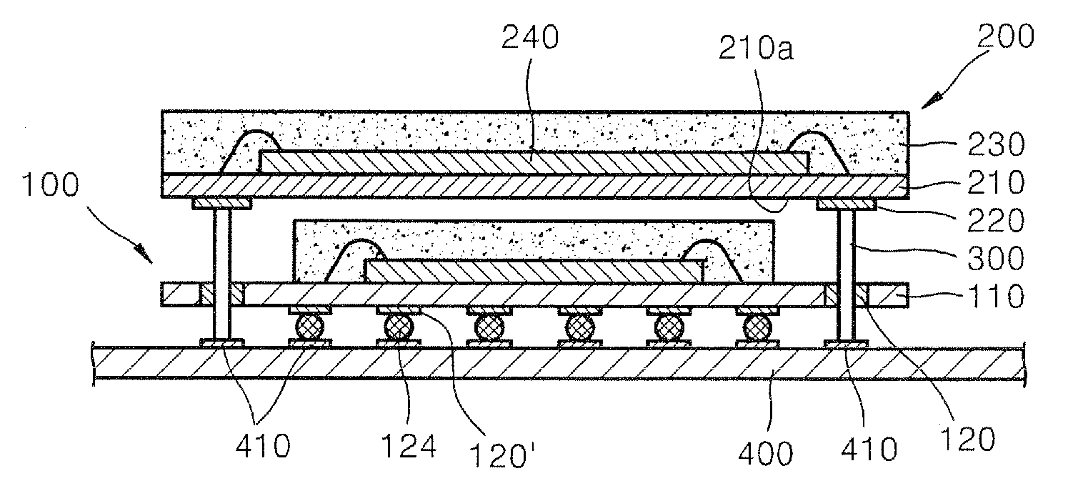
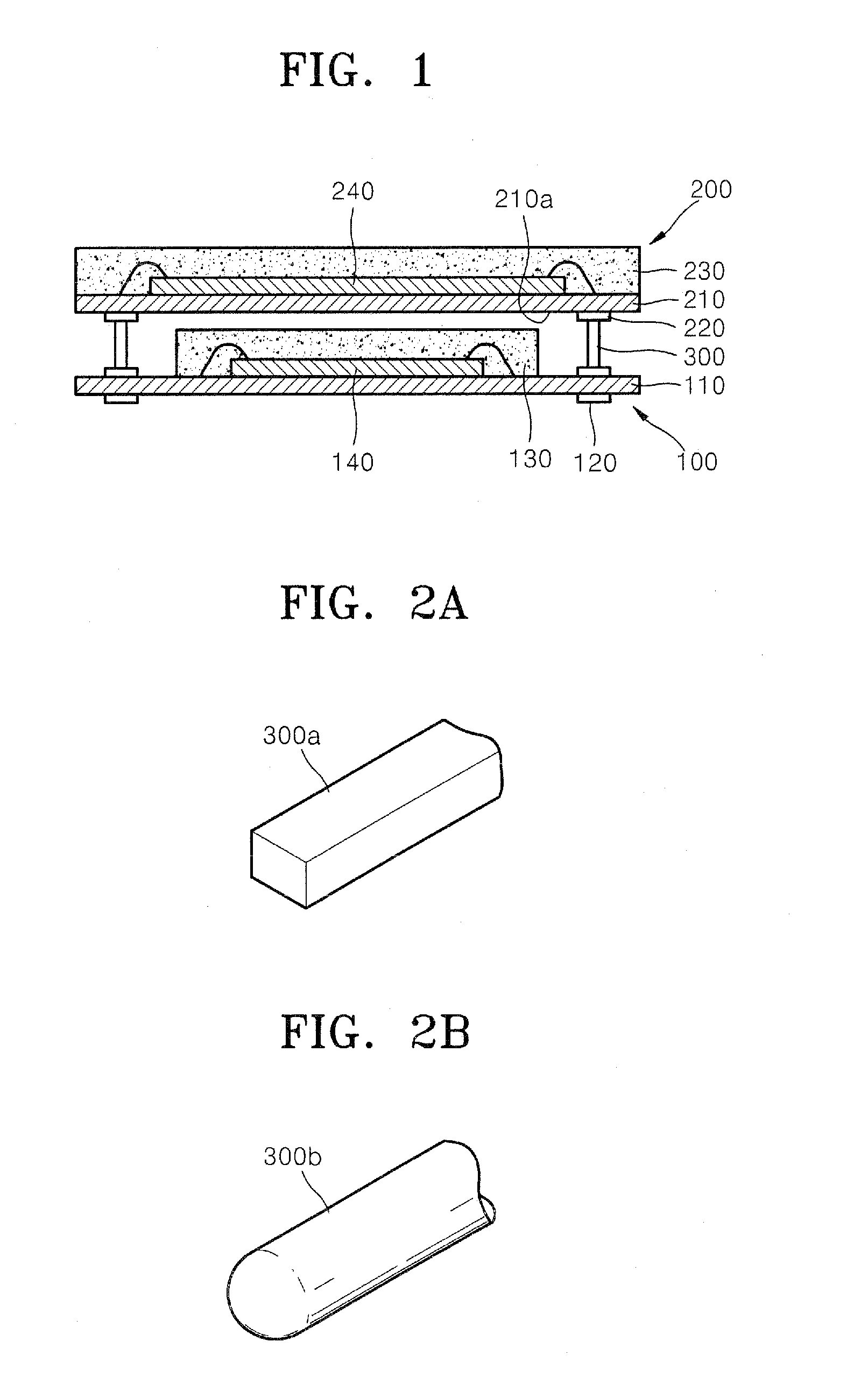
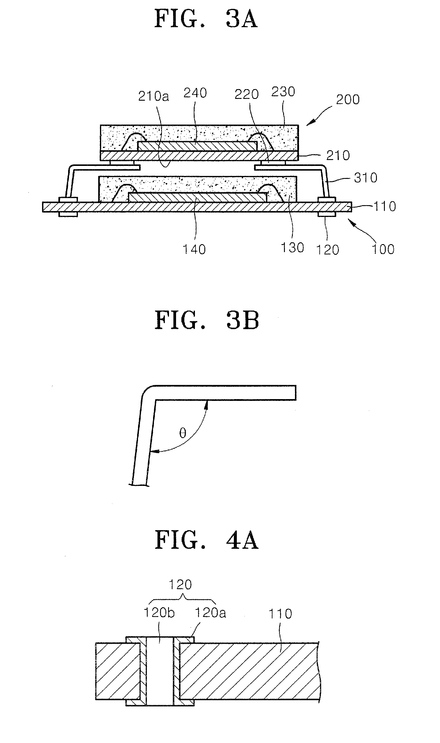
[0037]FIG. 1 illustrates a package-on-package (POP) package according to an embodiment of the present invention.

[0038]A POP package according to an embodiment of the present invention includes a first semiconductor package 100 ...


PUM


Abstract

A package-on-package (POP) package in which semiconductor packages are stacked using lead lines rather than conventional solder balls, and a fabricating method thereof are provided. According to the POP package and the fabricating method thereof of the present invention, the POP package is prevented from being short-circuited even when an underlying semiconductor package gets thicker and the POP package can sufficiently withstand deformation caused by post-fabrication warpage.

Description

CROSS-REFERENCE TO RELATED APPLICATION[0001]This application claims priority under 35 U.S.C. § 119 to Korean Patent Application No. 10-2006-0085881, filed on Sep. 6, 2006, in the Korean Intellectual Property Office, the disclosure of which is incorporated herein in its entirety by reference.BACKGROUND[0002]1. Technical Field[0003]The present invention relates to a package-on-package (POP) package and a fabricating method thereof, and more particularly, to a POP package which is prevented from being short-circuited even when an underlying semiconductor package is thick and which can sufficiently withstand deformation caused by post-fabrication warpage, and a fabricating method thereof.[0004]2. Description of the Related Art[0005]In recent years, as electronic products have been incorporating greater functionality, a number of devices need to be integrated in one substrate, which makes it difficult to achieve the desired compactness of the products. Accordingly, researchers are curren...

Claims


Application Information

Patent Timeline
Patent Type & Authority Applications(United States)
IPC IPC(8): H01L23/52H01L21/00
CPCH01L23/49811H01L25/105H01L2225/1023H01L2924/3511H01L2224/73265H01L2224/32225H01L2224/32145H01L24/48H05K2201/10946H05K2201/10734H05K2201/10704H05K2201/10689H05K2201/10515H05K3/3447H05K3/3421H05K1/181H01L2224/48091H01L2224/48225H01L2224/48227H01L2225/06568H01L2924/15311H01L2924/15331H01L2924/00014H01L2924/00012H01L2924/00H01L24/73H01L2924/181Y02P70/50H01L2224/45099H01L2224/45015H01L2924/207H01L23/12
Inventor HWANG, SUNG-WOOK
Owner SAMSUNG ELECTRONICS CO LTD
Why Eureka
Try Eureka