Semiconductor integrated device and manufacturing method for the same

a technology of integrated devices and semiconductors, which is applied in the direction of semiconductor devices, electrical devices, transistors, etc., can solve the problems of affecting the stability of the potentiometer and the latching problem, and achieve the effect of reducing the size of the integrated device, preventing latching, and low resistan

Inactive Publication Date: 2009-06-04
RENESAS ELECTRONICS CORP
View PDF14 Cites 0 Cited by
  • Summary
  • Abstract
  • Description
  • Claims
  • Application Information

AI Technical Summary

Benefits of technology

[0010]According to the semiconductor integrated device of the present invention, the potential of the first wells of the first conductivity type and the potential of the second wells of the second conductivity type are supplied respectively via the impurity layer of the first conductivity type and the impurity layer of the second conductivity type that are high in impurity concentration from below each well. These two layers form well potential supply lines of low resistance and hence can stably supply well potentials to the wells of the same conductivity types.
[0011]In the semiconductor integrated device of the present invention, via the two impurity layers of high concentration under the wells, the wells of the same conductivity types are stably supplied with potentials, and hence latch-up can be prevented not depending on the resistance of the semiconductor substrate. Thus, it is possible to achieve the reduction in size of the semiconductor integrated device by reducing the number of the tap areas via which to supply well potentials and at the same time to prevent the occurrence of latch-up.

Problems solved by technology

With the technique disclosed in the above-cited Japanese Unexamined Patent Application Publication, it is possible to reduce semiconductor integrated devices in size, but because the potential of wells of the same conductivity type as the semiconductor substrate is supplied via the semiconductor substrate, the potential may not be stably supplied depending on the resistance of the semiconductor substrate.
Hence, the potential of the wells of the same conductivity type as the semiconductor substrate becomes unstable, and the problem of latch-up may occur.

Method used


Image

  • Semiconductor integrated device and manufacturing method for the same
  • Semiconductor integrated device and manufacturing method for the same
  • Semiconductor integrated device and manufacturing method for the same

Examples


Embodiment Construction

Embodiments of the Invention

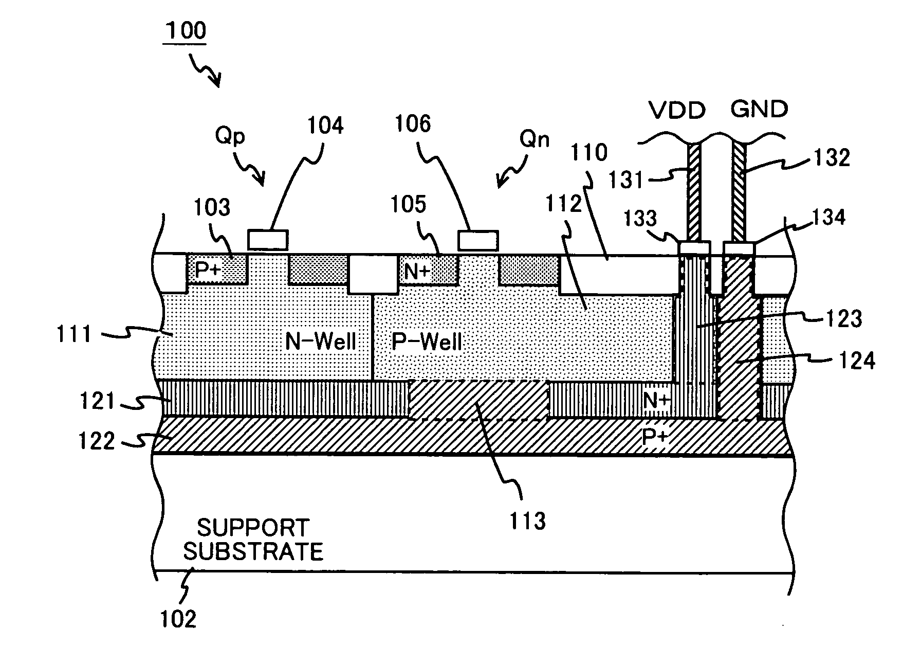
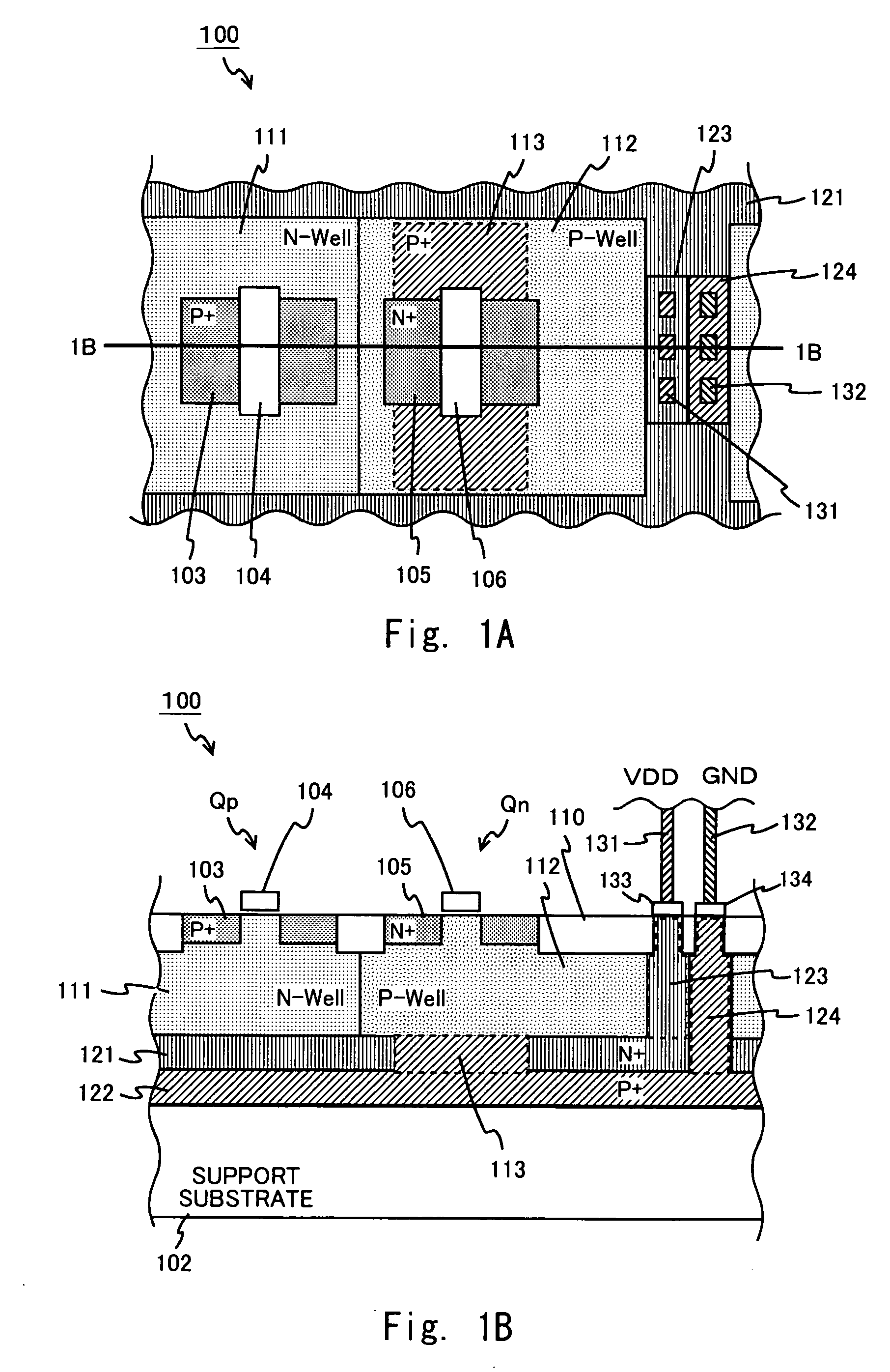
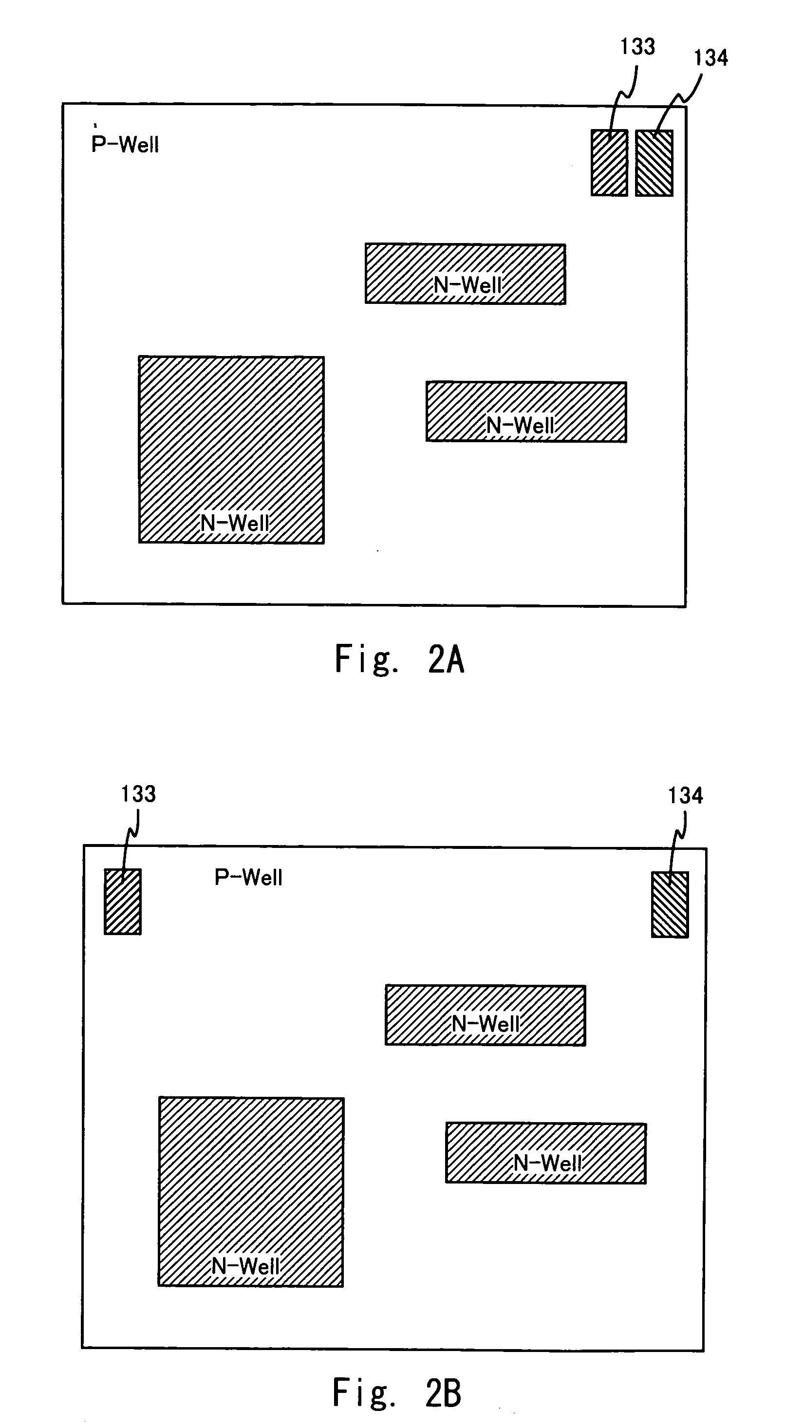
[0053]An embodiment of the present invention will be described below with reference to the drawings. FIGS. 1A and 1B are a plan view and a sectional view of a semiconductor integrated device 100 according to the present embodiment. FIG. 1A is a plan view of the semiconductor integrated device 100, and FIG. 1B is a sectional view taken along line 1B-1B of FIG. 1A. Note that element separation regions 110 described later are omitted in FIG. 1A.

[0054]As shown in FIGS. 1A, 1B, the semiconductor integrated device 100 comprises a support substrate 102, second wells 111 of a second conductivity type (hereinafter referred to as N-type wells), first wells 112 of a first conductivity type (hereinafter referred to as P-type wells), a second impurity layer 121 of the second conductivity type that is higher in impurity concentration than the N-type well 111 (hereinafter referred to as an N-type impurity layer), and a first impurity layer 122 of the first conductivity ...


PUM


Abstract

A first exemplary aspect of an exemplary embodiment of the present invention is a semiconductor integrated device comprising a semiconductor substrate, a first impurity layer of a first conductivity type formed in the semiconductor substrate, a second impurity layer of a second conductivity type formed on the first impurity layer, a first well of the first conductivity type formed on the second impurity layer and supplied with potential from the first impurity layer via an impurity region of the first conductivity type selectively formed in a part of the second impurity layer, and a second well of the second conductivity type formed on the second impurity layer and supplied with potential from the second impurity layer, wherein the impurity concentrations of the first impurity layer and the impurity region are higher than that of the first well, and the impurity concentration of the second impurity layer is higher than that of the second well.

Description

BACKGROUND[0001]1. Field of the Invention[0002]The present invention relates to a semiconductor integrated device and a manufacturing method for the same.[0003]2. Description of Related Art[0004]FIG. 22 shows a schematic view of a cross-section of a related-art typical semiconductor integrated device 1. As shown in FIG. 22, the semiconductor integrated device 1 has wells for PMOS transistors and NMOS transistors formed on a substrate 2. Each well has a tap 3 or 4 formed in its top. Lines 5, 6 via which to supply a power supply voltage VDD and ground voltage GND are connected to the taps 3, 4. By this means, ground voltage GND or power supply voltage VDD is supplied as a well potential to each well.[0005]Technology for reducing semiconductor integrated devices in size is disclosed in Japanese Unexamined Patent Application Publication No. 2007-5763. In this Japanese Unexamined Patent Application Publication, an N-type buried layer is positioned in a P-type semiconductor substrate, and...

Claims


Application Information

Patent Timeline
Patent Type & Authority Applications(United States)
IPC IPC(8): H01L29/02H01L21/04
CPCH01L21/743H01L21/823892H01L29/78H01L29/1087H01L27/0921
Inventor OKAMOTO, HITOSHI
Owner RENESAS ELECTRONICS CORP
Why Eureka
Try Eureka