Touch screen panel and method for manufacturing the same

a technology of touch screen and manufacturing method, which is applied in the field of touch screen panels, can solve the problems of reducing the luminance of the display, increasing the thickness of the lcd device, and high cost of the touch screen pad, and achieves the reduction of the thickness and the number of manufacturing processes of the touch screen panel. , the effect of reducing the manufacturing cos

Inactive Publication Date: 2008-03-06
SAMSUNG ELECTRONICS CO LTD
View PDF4 Cites 97 Cited by
  • Summary
  • Abstract
  • Description
  • Claims
  • Application Information

AI Technical Summary

Benefits of technology

[0023] According to the touch screen panel and the method for manufacturing the touch screen panel, a plurality of hall sensing parts is formed in pixel parts to detect a position of a magnetic member that approaches or is contacted to the touch screen panel from the exterior, so that the conventional touch screen pad may be omitted. Therefore, manufacturing costs, thickness and the number of manufacturing processes of the touch screen panel may be reduced.

Problems solved by technology

However, the cost of the touch screen pad is high and, and increases the thickness of the LCD device as well as reducing the luminance of the display.

Method used


Image

  • Touch screen panel and method for manufacturing the same
  • Touch screen panel and method for manufacturing the same
  • Touch screen panel and method for manufacturing the same

Examples


Embodiment Construction

[0033] It will be understood that when an element or layer is referred to as being “on,”“connected to” or “coupled to” another element or layer, it can be directly on, connected or coupled to the other element or layer or intervening elements or layers may be present. In contrast, when an element is referred to as being “directly on,”“directly connected to” or “directly coupled to” another element or layer, there are no intervening elements or layers present.

[0034] Hereinafter, the present invention will be described in detail with reference to the accompanying drawings.

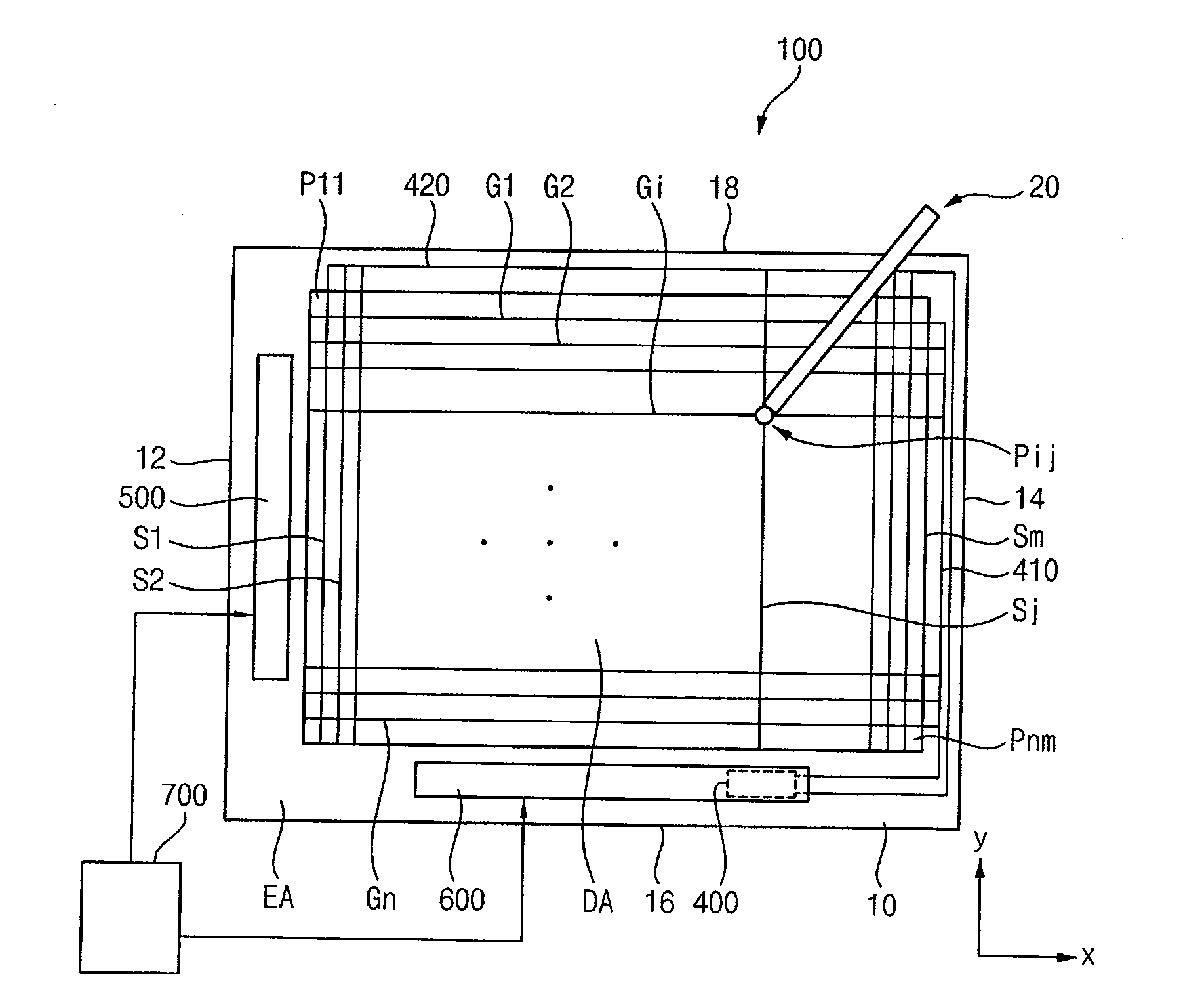
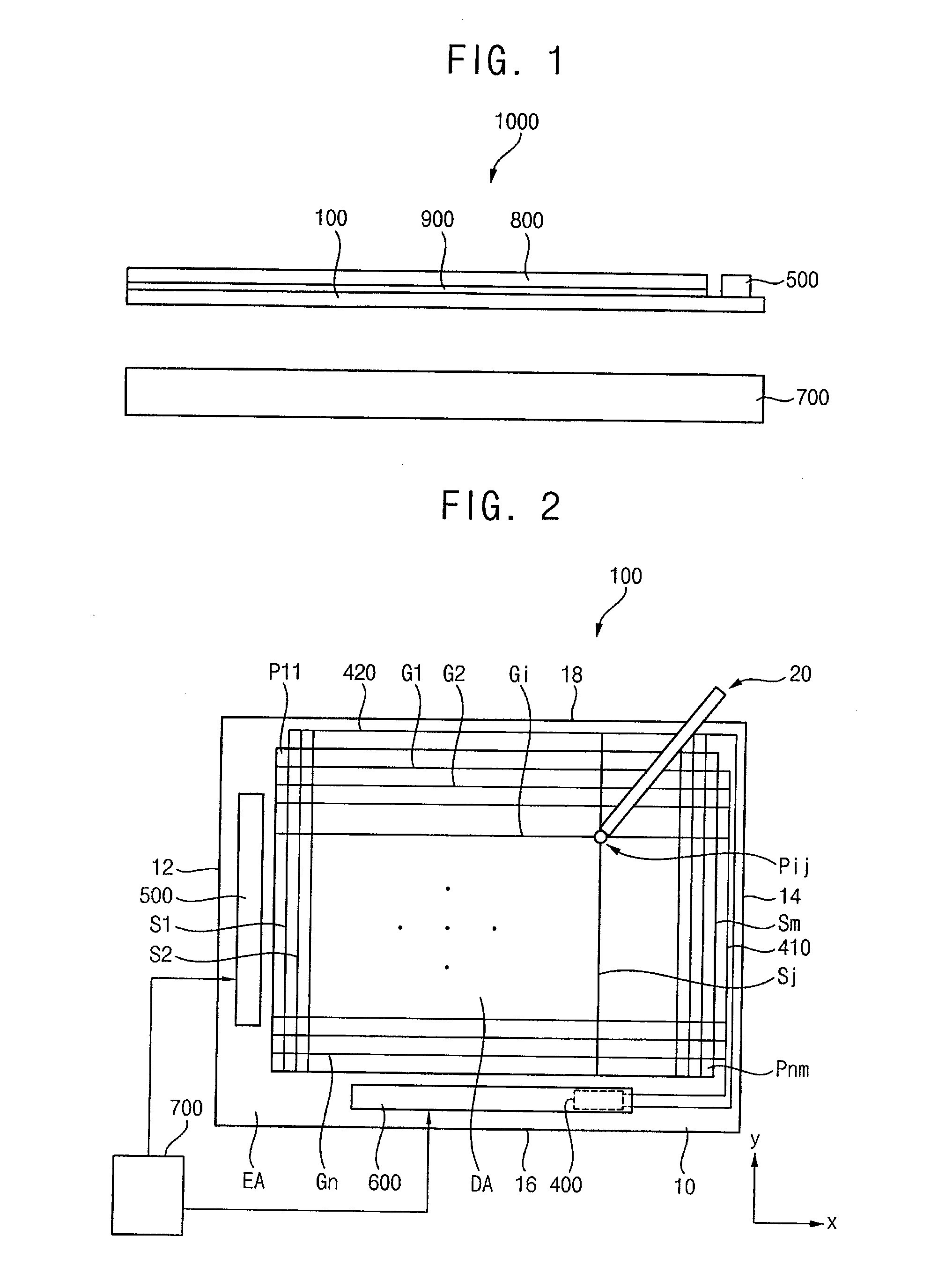
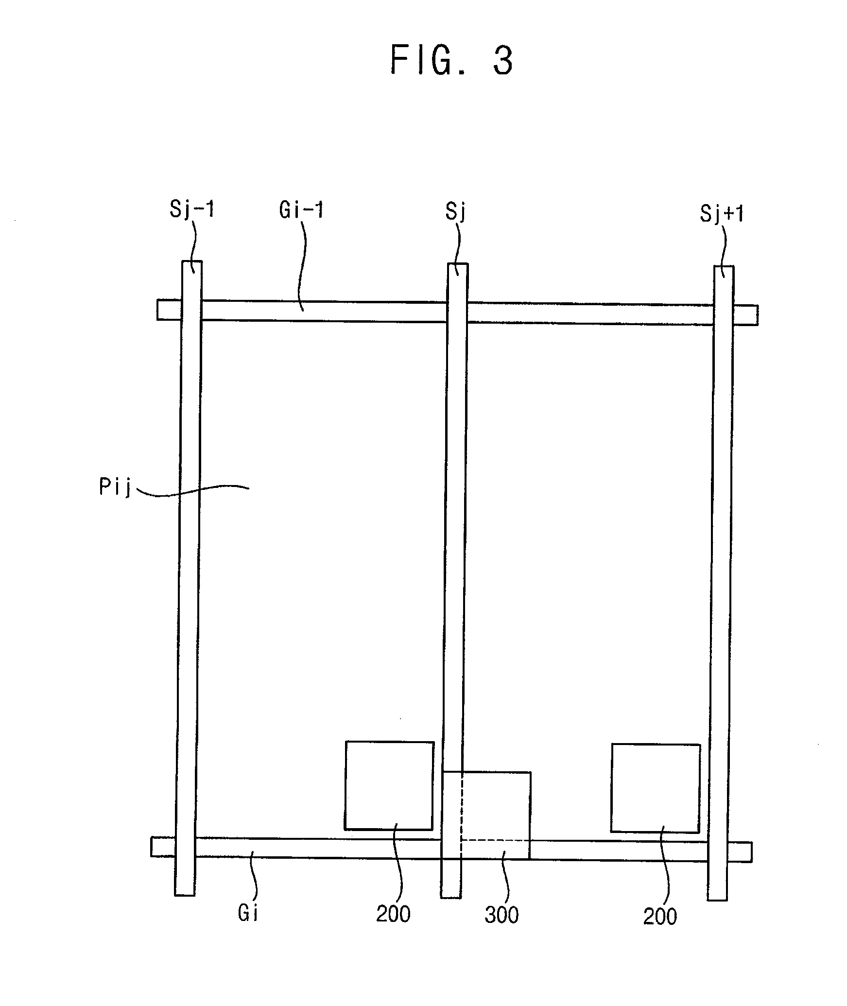
[0035]FIG. 1 is a side view illustrating a touch screen panel according to an exemplary embodiment of the present invention. FIG. 2 is a plan view illustrating the display substrate in FIG. 1. FIG. 3 is a partially enlarged plan view illustrating a pixel part in FIG. 2.

[0036] Referring to FIGS. 1 to 4, a touch screen panel 1000 according to an exemplary embodiment of the present invention includes a display substr...


PUM


Abstract

A plurality of pixel parts is electrically connected to gate and source lines. Each of the pixel parts has a thin-film transistor (TFT) formed therein. A plurality of hall sensing parts is formed in the pixel parts. A plurality of hall sensing parts varies a reference current applied to the gate and the source lines by a magnetic member. The position detector is electrically connected to the gate lines and the source lines. The position detector detects a position of the magnetic member using the gate and source lines to which a varied current is applied. The plurality of hall sensing parts formed in the pixel parts detect the position of the magnetic member that approaches or contacts the screen of the display.

Description

CROSS-REFERENCE TO RELATED APPLICATIONS [0001] This application claims priority under 35 U.S.C. § 119 to Korean Patent Application No. 2006-83960 filed on Sep. 1, 2006 and Korean Patent Application No. 2007-19564 filed on Feb. 27, 2007 in the Korean Intellectual Property Office (KIPO), the contents of which are herein incorporated by reference in their entireties. BACKGROUND OF THE INVENTION [0002] 1. Field of the Invention [0003] The present invention relates to a touch screen panel and, more particularly, to a touch screen panel used for a display device and a method for manufacturing the touch screen panel. [0004] 2. Description of the Related Art [0005] Generally, a liquid crystal display (LCD) device includes an LCD panel including a display substrate having a plurality of thin-film transistors (TFTs) formed in a matrix shape to display an image, an opposing substrate facing the display substrate and a liquid crystal layer interposed between the display substrate and the opposi...

Claims


Application Information

Patent Timeline
Patent Type & Authority Applications(United States)
IPC IPC(8): G06F3/041G09G3/36
CPCG06F3/0412
Inventor YOO, DAN-SIKKATAKURA, TERUOKANG, CHANG-WOOK
Owner SAMSUNG ELECTRONICS CO LTD
Why Eureka
Try Eureka