Electrical conductivity bridge in a conductive multilayer article

a multi-layer, electrical conductivity technology, applied in the direction of printed circuit manufacturing, printed element electric connection formation, solid-state devices, etc., can solve the problem of producing more complex arrays of circuit paths with fewer layers of substrate material

Inactive Publication Date: 2008-03-06
KIMBERLY-CLARK WORLDWIDE INC
View PDF50 Cites 34 Cited by
  • Summary
  • Abstract
  • Description
  • Claims
  • Application Information

AI Technical Summary

Problems solved by technology

Additionally, more complex arrays of circuit-paths...

Method used


Image

  • Electrical conductivity bridge in a conductive multilayer article
  • Electrical conductivity bridge in a conductive multilayer article
  • Electrical conductivity bridge in a conductive multilayer article

Examples


examples 1-3

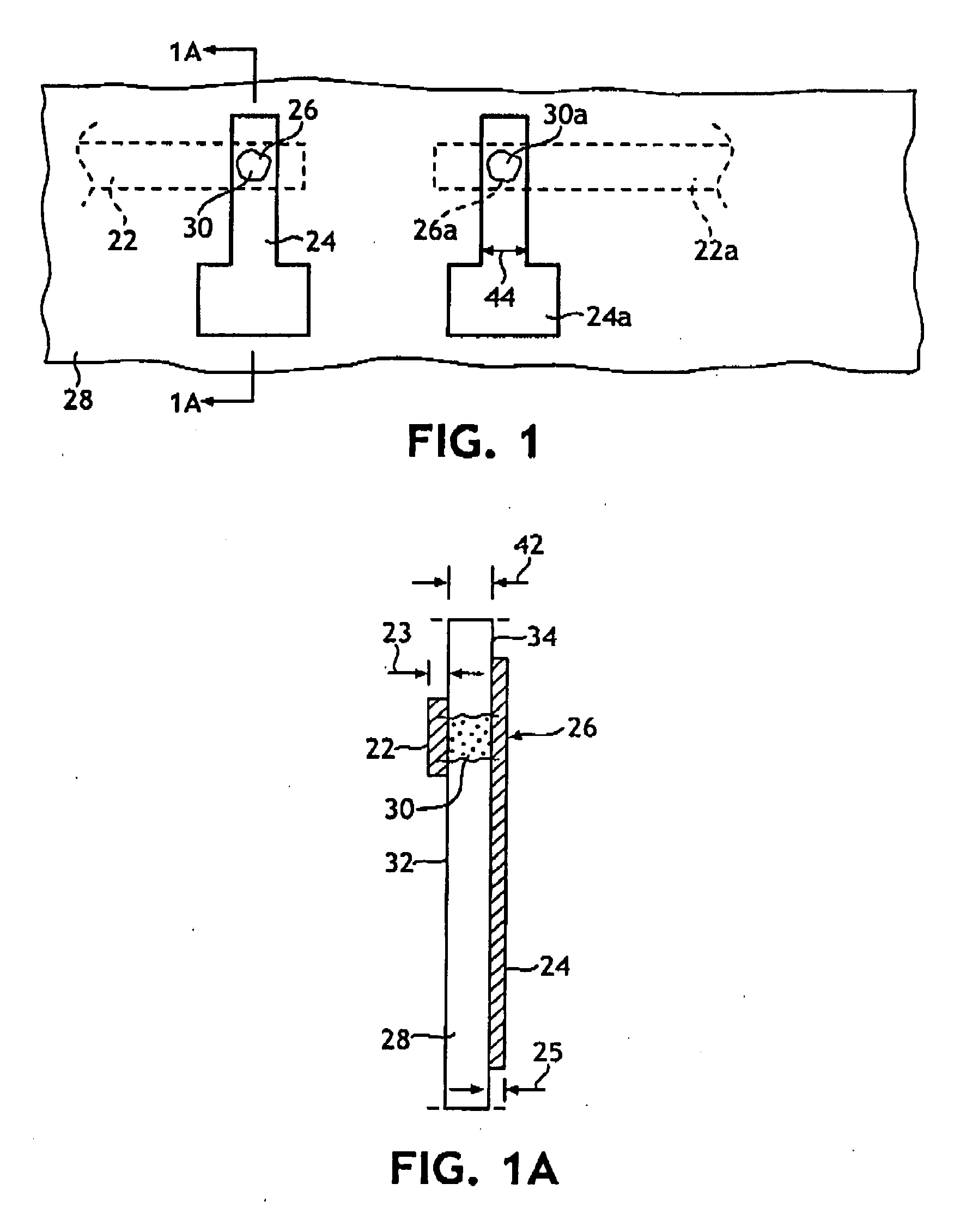
[0105]A first material was a composite film composed of 12 μm thick polyester substrate layer and a first circuit-path provided by a 12 μm thick aluminum foil. It is believed that the 12 μm thick aluminum circuit-path could be readily provided by printing a conductive aluminum ink onto the polyester substrate. A second material was composed of 0.75 mil (0.00075 inch) thick poly film with a second, 100 nm thick copper circuit-path printed on one side of the film.

[0106]Prior to bonding, the materials were arranged such that the copper circuit-path was on one side of the 0.75 mil poly film, and the aluminum circuit-path was against an opposite side of the 0.75 mil poly film. The aluminum circuit-path was operatively aligned with the copper circuit-path, and the aluminum foil material was bonded to the printed-copper circuit-path through the thickness of the 0.75 mil poly film. A BRANSON ultrasonic bonder Model 931 was used to bond the samples. The 20 kHz bonder was set at a 50 PSI bond...


PUM


Abstract

A method comprises providing a first electrically-conductive circuit-path (22), and separately providing a second electrically-conductive circuit-path (24). A portion of the first circuit-path is positioned proximally adjacent a portion of the second circuit-path at a first predetermined electrical bond location (26). A first, electrically-insulating barrier layer (28) is interposed between the first circuit-path and second circuit-path at the first bond location, and the first circuit-path is mechanically bonded to the second circuit-path at the first bond location. The mechanical bonding configured to provide an electrically-conductive bond-path between the first circuit-path and the second circuit-path at the first bond location. The mechanical bonding may desirably include ultrasonic bonding and/or pressure bonding.

Description

FIELD OF THE INVENTION[0001]The present invention relates to a method for interconnecting electrical circuits. More particularly, the present invention pertains to a technique for interconnecting electrical circuits through the thickness of an electrically insulating layer.BACKGROUND OF THE INVENTION[0002]Electrical circuits have been printed or otherwise applied to flexible substrates, such as paper, woven fabrics, nonwoven fabrics and polymer films. The electrical circuits have incorporated electrically-conductive inks applied with conventional ink-printing techniques and various products, such as badges, labels and tags, have incorporated the printed circuits. In particular arrangements, the printed circuits have been employed in hygienic products, such as drapes, gowns, garments, personal care absorbent products, and the like. In other arrangements, electrical / electronic circuitry has been employed to provide sensors located in selected personal care products, such as wetness se...

Claims


Application Information

Patent Timeline
IPC IPC(8): H01L21/44
CPCA61F13/42H01L2924/01037H01L2924/01078H01L2924/01079H01L2924/14H01L2924/19041H01L2924/19042H01L2924/19043H01L2924/30105H01L2924/30107H05K3/328H05K3/4084H05K2203/0285H05K2203/1189H01L2924/01019H01L24/72H05K1/11H05K3/40
Inventor TIPPEY, DAROLD DEANALES, THOMAS MICHAELEHLERT, THOMAS DAVID
Owner KIMBERLY-CLARK WORLDWIDE INC
Why Eureka
Try Eureka