Semiconductor light emitting device

a light-emitting device and semiconductor technology, applied in the direction of lasers, optical resonator shape and construction, semiconductor lasers, etc., can solve the problems of unnecessarily complicated fabrication process, and inability to meet the needs of electrical conta

Active Publication Date: 2008-03-13
HONG KONG APPLIED SCI & TECH RES INST
View PDF7 Cites 69 Cited by
  • Summary
  • Abstract
  • Description
  • Claims
  • Application Information

AI Technical Summary

Problems solved by technology

Furthermore, the disposal of the reflector between the light-emitting region and the conductive holder may make the fabrication process unnecessarily complicated.
However, the process of forming the Photonic Band Gap structure may be unnecessarily complicated.
Furthermore, the etching process may cause damages to the contact layer above the semiconductor cladding layer and consequently may make the electrical contact instable.

Method used


Image

  • Semiconductor light emitting device
  • Semiconductor light emitting device
  • Semiconductor light emitting device

Examples


Embodiment Construction

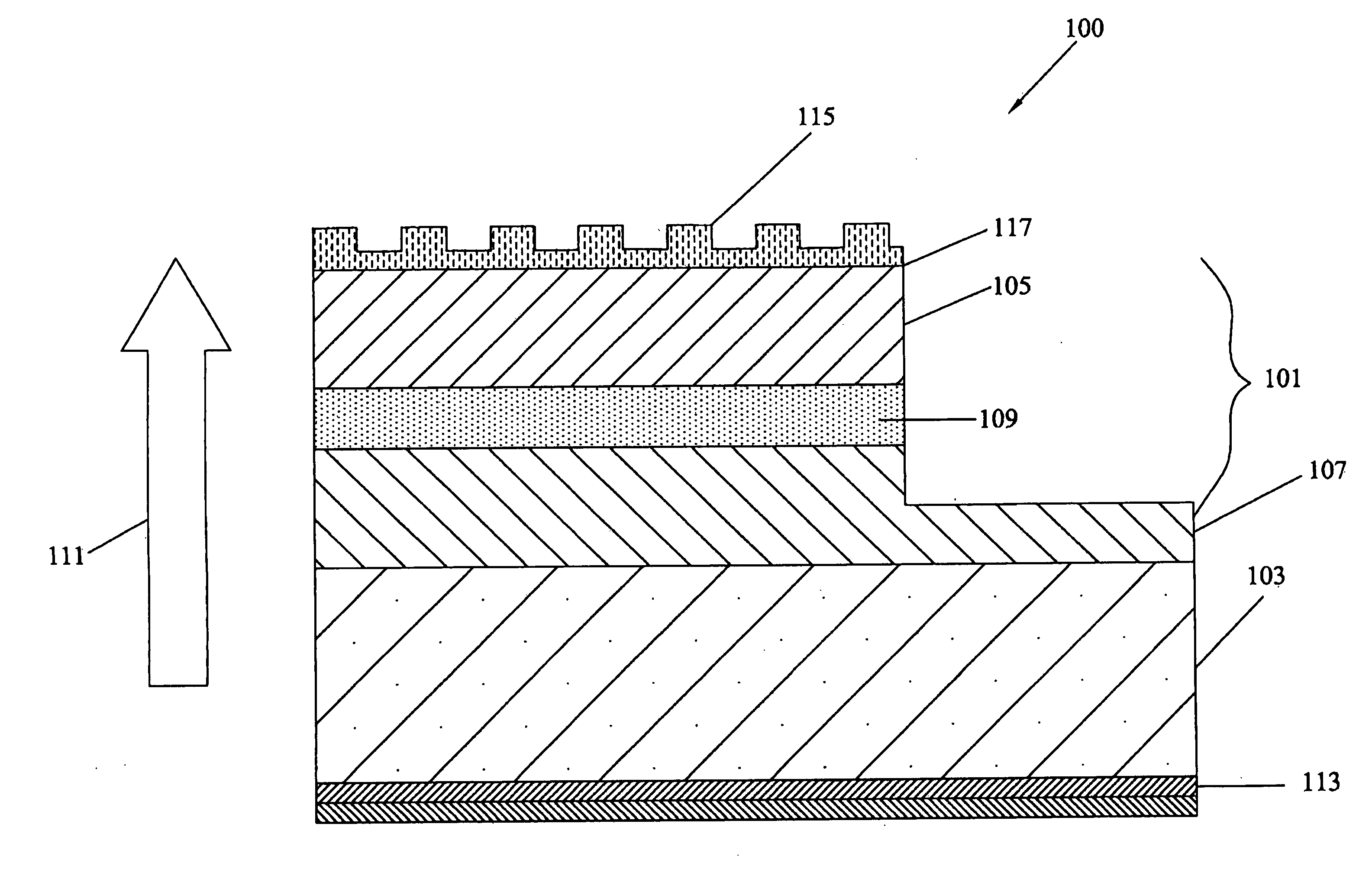
[0028]The following description refers to exemplary embodiments of a semiconductor light emitting assembly according to the present invention. Reference is made in the description to the accompanying drawings whereby the semiconductor light emitting assembly is illustrated in the exemplary embodiments. Similar components between the drawings are identified by the same reference numerals.

[0029]In FIG. 1, an exemplary embodiment of a top-emitting semiconductor light emitting device 100 includes a multi-layer stack 101 of materials formed on a substrate 103; the multi-layer stack 101 includes a layer of p-doped material or p-type semiconductor layer 105, a layer of n-doped material or an n-type semiconductor layer 107, and a light generating region or p-n junction 109 as generally understood in the art. When powered, the p-n junction 109 emits lights in all directions, but a primary amount of light emissions will exit the top-emitting semiconductor light emitting device 100 in a primar...


PUM


Abstract

A semiconductor light emitting device for emission of light having a predetermined bandwidth in a primary direction of emission includes a light generating region for the generation of light; and a 1-dimensional photonic crystal structure having a photonic bandgap covering at least a segment of said bandwidth. The 1-dimensional photonic crystal structure is located such that upon incident of light from the light generating region, light having a wavelength within the bandgap of the 1-dimensional photonic crystal structure is reflected in the primary direction of emission.

Description

FIELD OF THE INVENTION[0001]The present invention relates to the structure and fabrication of semiconductor light emitting devices. More particularly, the present invention relates to improvements in light emission efficiency of semiconductor light emitting devices.BACKGROUND OF THE INVENTION[0002]Light emitting diodes (LEDs) are semiconductor light emitting devices that emit lights when an electrical current is supplied thereto. Typically, an LED is formed of multiple layers of materials having a layer of p-doped material or p-type semiconductor layer (“p-layer”), a layer of n-doped material or an n-type semiconductor layer (“n-layer”), and a light generating region or p-n junction. When powered, the p-n junction emits lights in a primary direction towards one of the p- and n-layers creating a field of illumination.[0003]To improve light emission efficiency of an LED device, various techniques have been proposed by the prior art, examples of which follow.[0004]U.S. Pat. No. 6,784,4...

Claims


Application Information

Patent Timeline
Patent Type & Authority Applications(United States)
IPC IPC(8): H01L33/00H01L33/40H01L33/44
CPCH01L33/405H01L2933/0083H01L33/44
Inventor HUANG, YANCHIU, KUO-ANPENG, HUA-JUNFENG, JIANCHU, HUNG-SHEN
Owner HONG KONG APPLIED SCI & TECH RES INST
Why Eureka
Try Eureka