Electro-optical device and electronic apparatus

Active Publication Date: 2008-03-13
138 EAST LCD ADVANCEMENTS LTD
View PDF5 Cites 8 Cited by
  • Summary
  • Abstract
  • Description
  • Claims
  • Application Information

AI Technical Summary

Benefits of technology

[0016]An advantage of some embodiments of the invention is that it provides an electro-optical device and an electronic apparatus that are able to suppress defective display by reliably shielding light from entering transistors formed on a first substrate, while reducing variation in aperture ratio among pixels in the display area by using light shielding films formed on a second substrate and also preventing variation in pixel aperture ratio among liquid crystal devices, even when a positional deviation of the second substrate occurs relative to the first substrate in a bonding process.

Problems solved by technology

Here, when light enters known semiconductor layers in the transistors, specifically, channel regions of the semiconductor layers or regions of the semiconductor layers, which are electrically connected to pixel electrodes, the transistors malfunction and, therefore, there is a problem that display chrominance nonuniformity, cross-talk, and / or flicker occur in the liquid crystal device due to off leakage current and, in addition, defective display, such as a decrease in display contrast, occurs.
However, it is difficult to bond the opposite substrate to the element substrate with completely high positional accuracy.
Thus, there has been a problem that the pixel aperture ratio varies among liquid crystal devices.
In addition, there also has been a problem that the aperture ratio varies among pixels, in which some of the pixels ensure aperture ratios but other pixels have considerably decreased aperture ratios.
Thus, even when the second substrate is bonded to the first substrate with poor positional accuracy, that is, even when a positional deviation occurs, the island light shielding films, which slightly protrude into the light transmission regions of the pixels, reduce variation in aperture ratio among pixels in the display area of the electro-optical device and also prevent variation in pixel aperture ratio among liquid crystal devices.
On the other hand, when the width of each protruding portion is smaller than the line width of each scanning line, even when the second substrate is bonded to the first substrate with poor positional accuracy, the protruding portions that hardly protrude into the light transmission regions reliably reduce variation in aperture ratio among pixels in the display area of the electro-optical device.
On the other hand, when the width of each protruding portion is smaller than the line width of each second light shielding film formed on the first substrate, even when the second substrate is bonded to the first substrate with poor positional accuracy, the protruding portions that hardly protrude into the light transmission regions reliably reduce variation in aperture ratio among pixels in the display area of the electro-optical device.
Thus, even when the second substrate is bonded to the first substrate with poor positional accuracy, that is, even when a positional deviation occurs, the rectangular island light shielding films reduce variation in aperture ratio among pixels in the display area of the electro-optical device and also prevent variation in pixel aperture ratio among liquid crystal devices.
Thus, even when the second substrate is bonded to the first substrate with poor positional accuracy, that is, even when a positional deviation occurs, the island light shielding films which slightly protrude into the light transmission regions of the pixels, reduce variation in aperture ratio among pixels in the display area of the electro-optical device and also prevent variation in pixel aperture ratio among liquid crystal devices.

Method used


Image

  • Electro-optical device and electronic apparatus
  • Electro-optical device and electronic apparatus
  • Electro-optical device and electronic apparatus

Examples


first embodiment

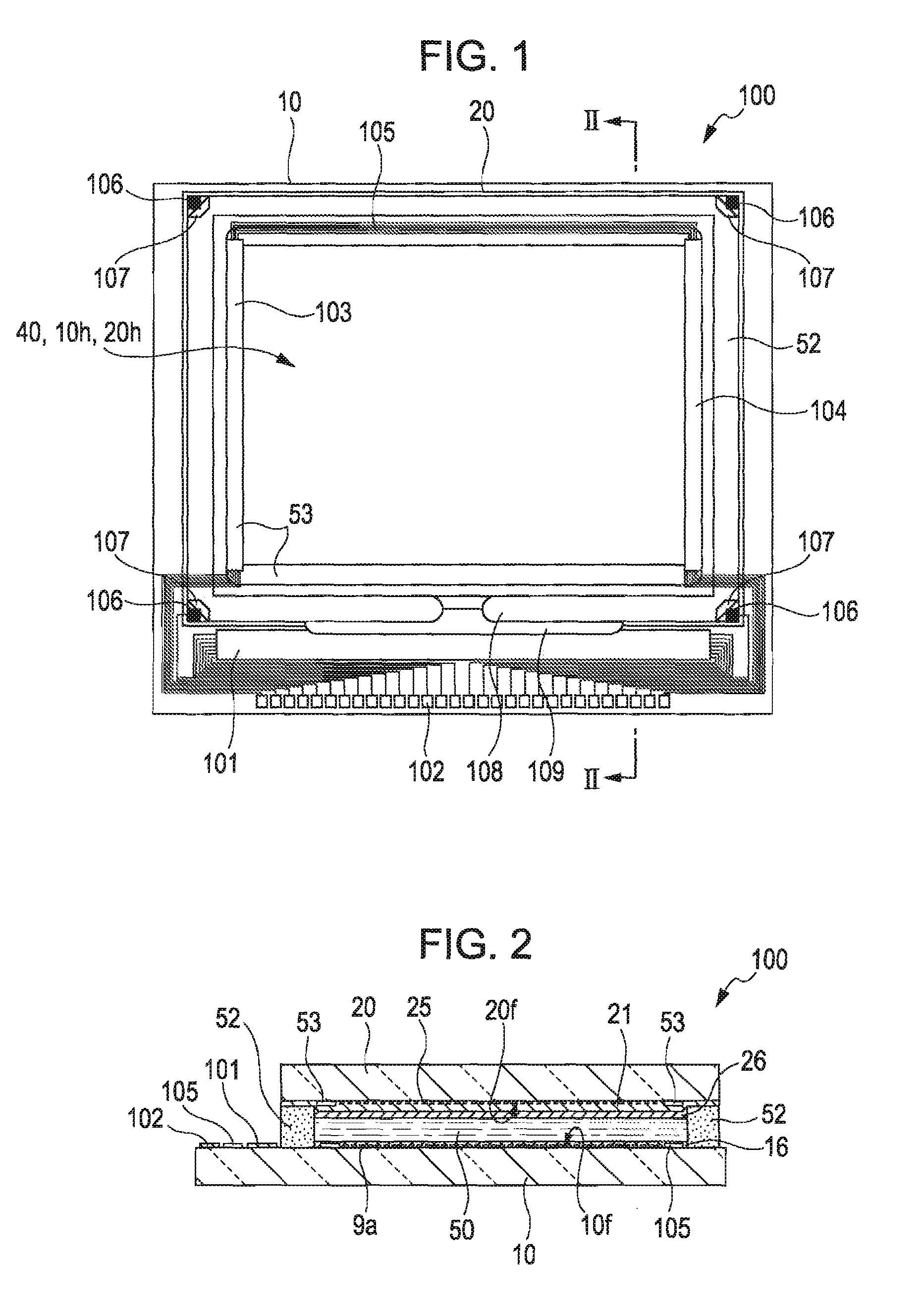
[0073]FIG. 1 is a plan view of a liquid crystal device according to the present embodiment. FIG. 2 is a cross-sectional view that is taken along line II-II in FIG. 1.

[0074]As shown in FIG. 1 and FIG. 2, a liquid crystal device 100, for example, includes a TFT substrate 10, an opposite substrate 20, and a liquid crystal 50. The TFT substrate 10 is formed of, for example, a crystal substrate, a glass substrate, or a silicon substrate. The opposite substrate 20 is opposed to the TFT substrate 10 and is formed of, for example, a glass substrate, a crystal substrate, or a silicon substrate. The liquid crystal 50, which is a electrooptic material, is interposed in a space between the TFT substrate 10 and the opposite substrate 20. The TFT substrate 10 and the opposite substrate 20, which are opposed to each other, are bonded by a seal material 52.

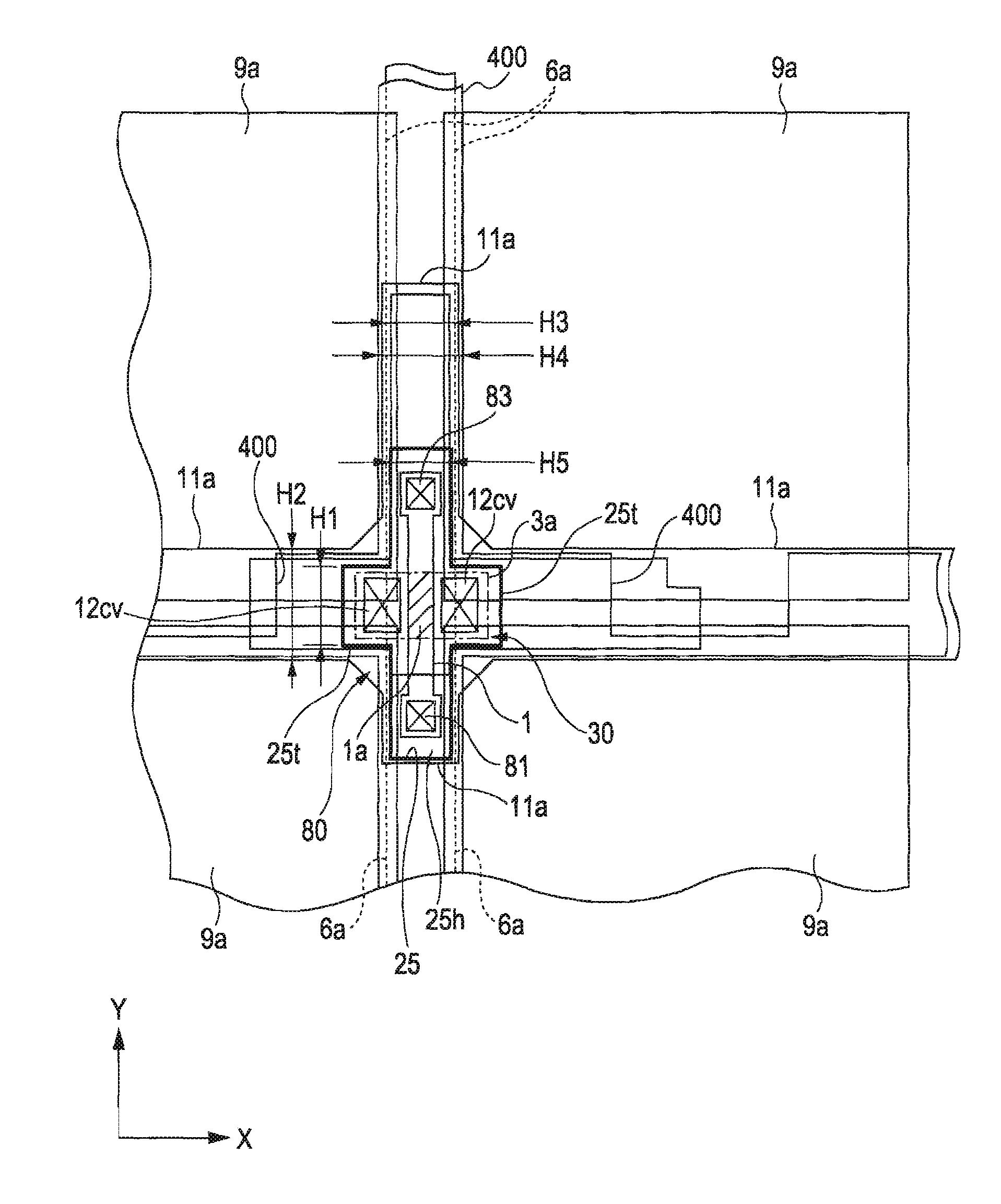
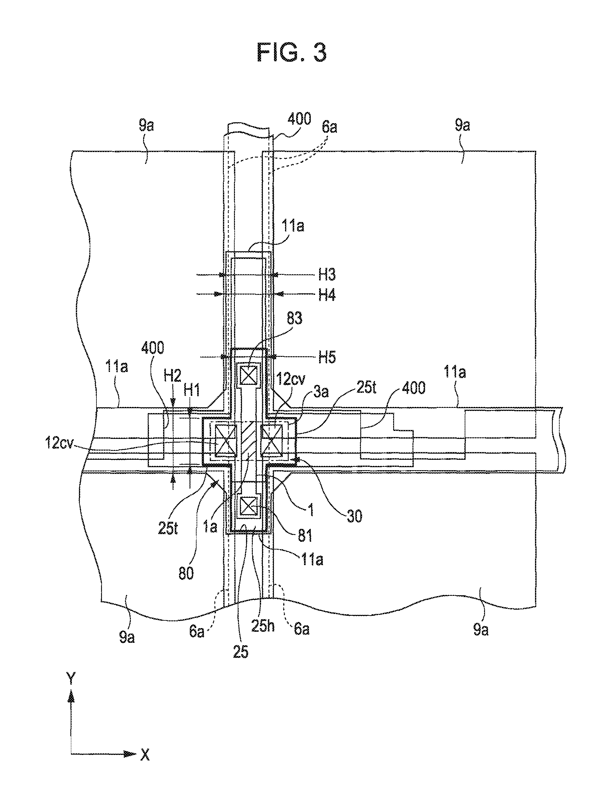
[0075]A display area 10h of the TFT substrate 10 which forms a display area 40 of the liquid crystal device 100 is formed on a surface 10f of th...

second embodiment

[0129]FIG. 7 is a partial plan view showing portion of a deposition pattern that is laminated on a TFT substrate and arrangement of one of BMs formed on an opposite substrate in a liquid crystal device according to the present embodiment.

[0130]The configuration of the liquid crystal device according to the second embodiment is only different from the liquid crystal device 100 according to the first embodiment in that the BM is formed into a rectangular shape on the opposite substrate 20. Thus, only the difference will be described, the same reference numerals are assigned to the same or similar components as those of the liquid crystal device 100 according to the first embodiment, and a description thereof is omitted.

[0131]As shown in FIG. 7, BMs 250 each are patterned in a corresponding one of the crossover regions 80 to form a rectangular island shape that at least partially overlaps the semiconductor layer 1 of the TFT 30 in plan view.

[0132]Specifically, in each of the crossover ...

third embodiment

[0147]FIG. 10 is a partial plan view showing portion of the lower layer of a deposition pattern that is laminated on a TFT substrate and arrangement of BMs formed on an opposite substrate in a liquid crystal device according to the present embodiment. FIG. 11 is a partial plan view showing portion of the upper layer of the deposition pattern that is laminated on the TFT substrate of the liquid crystal device according to the present embodiment. FIG. 12 is a cross-sectional view, taken along the line XII-XII in FIG. 10 and FIG. 11, showing the TFT substrate when the configurations shown in FIG. 10 and the configuration shown in FIG. 11 are laminated.

[0148]The configuration of the liquid crystal device according to the third embodiment is only different from the liquid crystal device 100 according to the first embodiment and the liquid crystal device according to the second embodiment in that, as viewed in plan, the shape of each scanning line and the shape of each island BM formed on...


PUM


Abstract

An electro-optical device includes semiconductor layers disposed between a first substrate and an electro-optical layer. The semiconductor layers are provided at positions corresponding to crossover regions of scanning lines and data lines. Island light shielding films are disposed between the second substrate and the electro-optical layer. The island light shielding films are isolated from each other and at least partially overlapping a corresponding one of the semiconductor layers in plan view.

Description

BACKGROUND[0001]1. Technical Field[0002]The present invention relates to an electro-optical device having a pair of first substrate and second substrate, which are opposed to each other, and light shielding films; which are formed on the second substrate to shield light from entering corresponding transistors formed on the first substrate, and also relates to an electronic apparatus having the electro-optical device.[0003]2. Related Art[0004]A known electro-optical device, such as a light transmissive liquid crystal device is configured so that liquid crystal is interposed between a first substrate and a second substrate, which are formed of a glass substrate, a crystal substrate, a silicon substrate, or the like. Switching elements, such as thin-film transistors, and pixel electrodes are arranged on the first substrate in a matrix and an opposite electrode is arranged on the second substrate. Then, image display may be performed by changing the optical characteristics of the liquid...

Claims


Application Information

Patent Timeline
IPC IPC(8): H01L31/0232
CPCG02F1/133512G02F2201/40G02F2001/133562G02F1/133562G02F1/1335
Inventor NAKAGAWA, MASASHI
Owner 138 EAST LCD ADVANCEMENTS LTD
Why Eureka
Try Eureka