Removing solution, cleaning method for semiconductor substrate, and process for production of semiconductor device

a cleaning method and technology for semiconductor substrates, applied in detergent compounding agents, manufacturing tools, inorganic non-surface active detergent compositions, etc., can solve problems such as damage to device reliability, and achieve the effect of preventing readhesion of removed metal contaminants and excellent ability for removal of metal contaminants

Inactive Publication Date: 2008-03-20
RENESAS ELECTRONICS CORP
View PDF19 Cites 5 Cited by
  • Summary
  • Abstract
  • Description
  • Claims
  • Application Information

AI Technical Summary

Benefits of technology

[0032] Thus, a cerium (IV) nitrate salt, periodic acid or a hypochlorite has an excellent ability for removal of metal contaminants containing copper, silver or palladium and further can effectively prevent readhesion of the removed metal contaminants. This is a new finding and the present invention has been completed based on the finding.

Problems solved by technology

In this case, however, sodium acts on the device region of semiconductor substrate and may damage the reliability of the device; therefore, care is preferably taken so that the removing solution does not act on the device-formed area.

Method used


Image

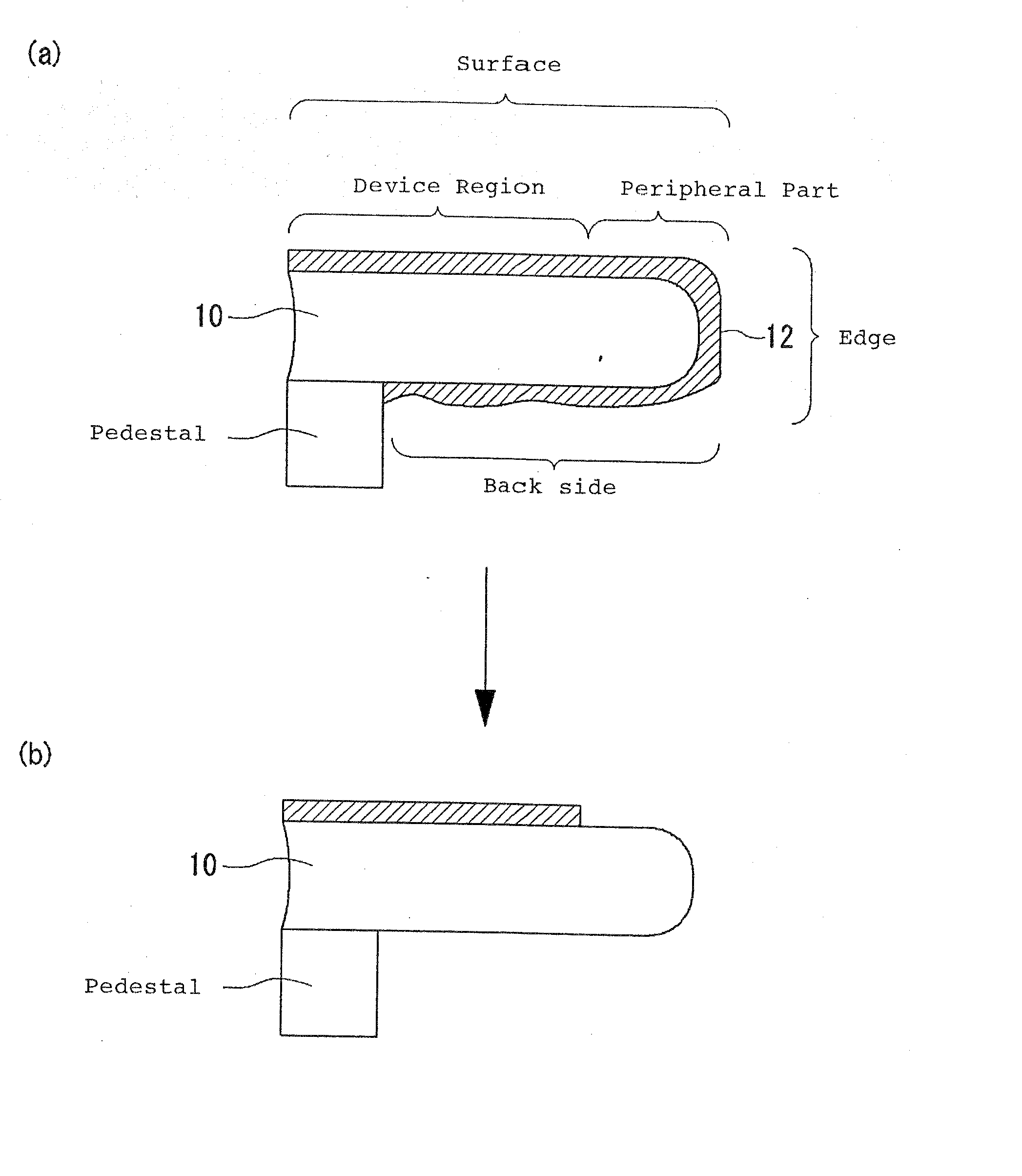
  • Removing solution, cleaning method for semiconductor substrate, and process for production of semiconductor device
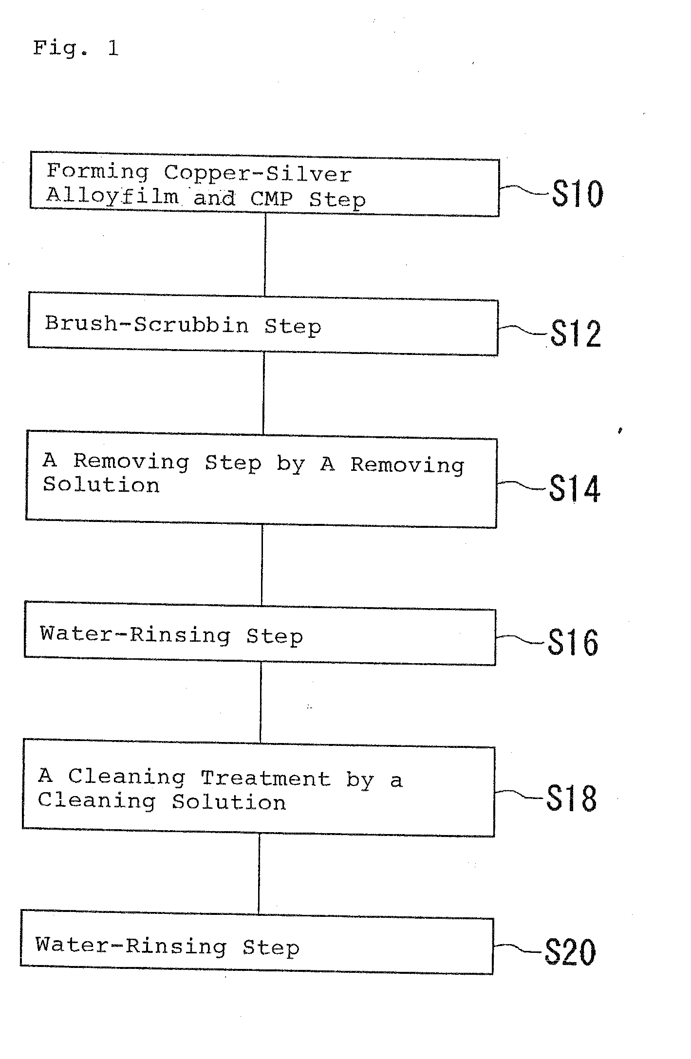
  • Removing solution, cleaning method for semiconductor substrate, and process for production of semiconductor device
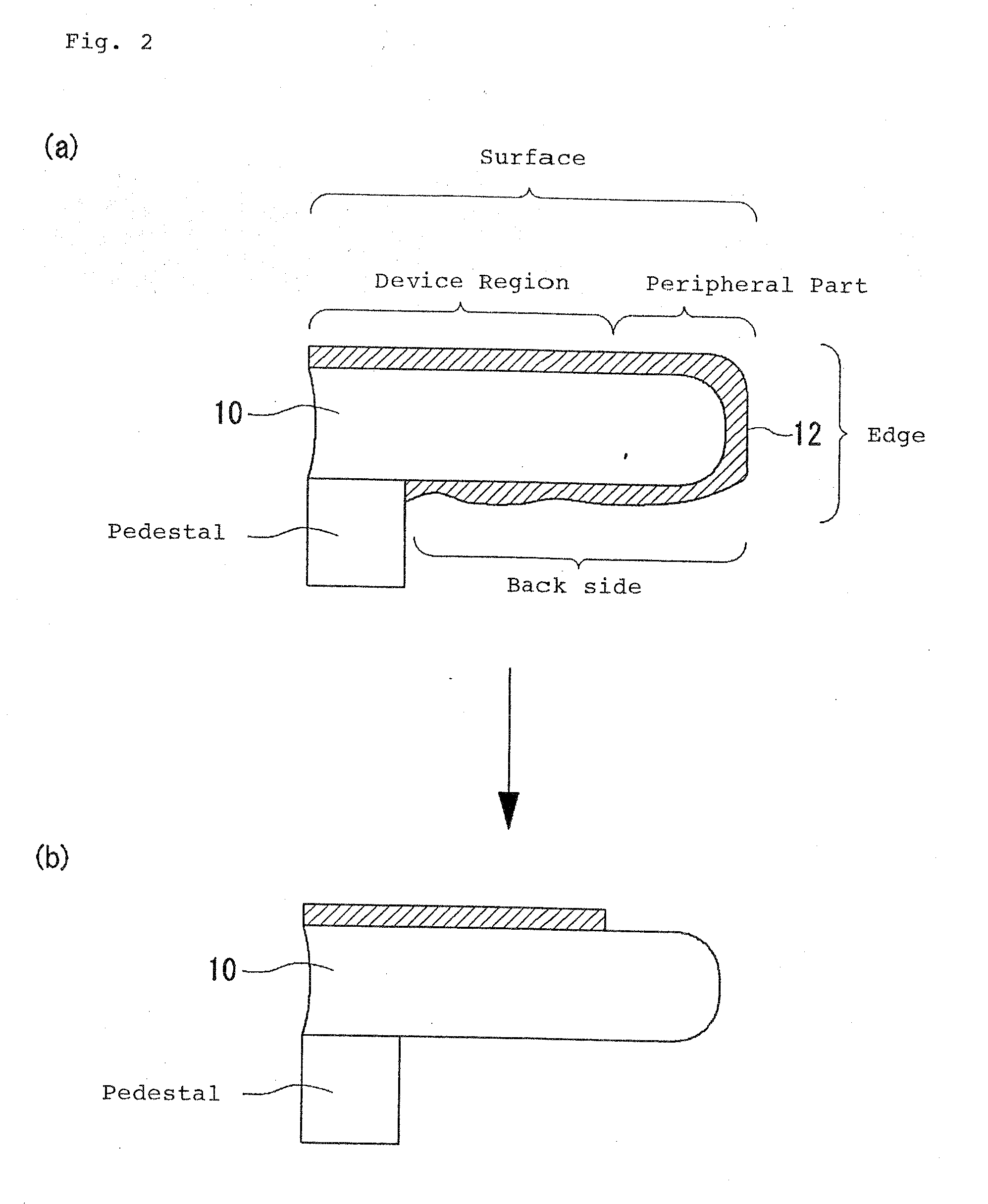
  • Removing solution, cleaning method for semiconductor substrate, and process for production of semiconductor device

Examples


reference example 1

[0073] A sample was spin-washed for 30 seconds using various removing solutions. In this Reference Example, removing solutions containing nitric acid were used. The compositions of the removing solutions used are shown in Table 2. The amounts of copper contaminant and silver contaminant remaining on a semiconductor substrate after the removing treatment were measured by fluorescent X-ray analysis. The results are shown also in Table 2. As shown in Table 1, the etching rates of copper and silver by nitric acid (70% by mass) are relatively high at 1 μm / min or more. That is, nitric acid (70% by mass) can dissolve the copper or silver layer formed in a process for semiconductor device production. Nevertheless, the removing solutions having compositions shown in Table 2 were unable to remove copper or silver.

TABLE 2×10¹⁰ atoms / cm2AgCuRemoving solutioncontaminationcontaminationBefore cleaning4329710951(a) HNO3 (1.4%)5921829(b) HNO3 (7%)5461764(c) HNO3 (20%)1505325(d) HNO3 (35%)406821(e)...

reference example 2

[0074] A sample was spin-washed for 30 seconds using various removing solutions. In this Reference Example, removing solutions containing sulfuric acid were used. The compositions of the removing solutions used are shown in Table 3. The amounts of copper contaminant and silver contaminant remaining on a semiconductor substrate after the removing treatment were measured by fluorescent X-ray analysis. The results are shown also in Table 3. Copper could not be removed with the removing solutions having compositions shown in Table 3, other than those shown in (i) and (k); and silver could not be removed with any removing solution.

TABLE 3×10¹⁰ atoms / cm2AgCuRemoving solutioncontaminationcontaminationBefore washing4329710951(h) H2SO4:H2O = 2:50649614(i) H2SO4:H2O2:H2O = 2:1:50564ND(j) H2SO4:H2O2:HF:H2O = 2:1:1:5037320117(k) H2SO4:H2O2:HF:H2O = 2:1:1:101253ND

reference example 3

[0075] A sample was spin-washed for 30 seconds using various removing solutions. In this Reference Example, removing solutions containing hydrofluoric acid were used. The compositions of the removing solutions used are shown in Table 4. The amounts of copper contaminant and silver contaminant remaining on a semiconductor substrate after the removing treatment were measured by fluorescent X-ray analysis. The results are shown also in Table 4. Copper could not be removed with the removing solutions having compositions shown in Table 4, other than that shown in (n); and silver could not be removed with any removing solution.

TABLE 4×10¹⁰ atoms / cm2AgCuRemoving solutioncontaminationcontaminationBefore washing4329710951(l)HF:HNO3:H2O = 1:5:2054918202(m) HF:H2O2:H2O = 1:5:100 (FPM)51010→ HF:HNO3:H2O = 1:5:20(n) HF:H2O2:H2O = 1:5:100 (FPM)2340ND


PUM

PropertyMeasurementUnit
temperatureaaaaaaaaaa
resistivityaaaaaaaaaa
temperatureaaaaaaaaaa

Abstract

The removing solution containing a cerium (IV) nitrate salt, periodic acid or a hypochlorite can be applied to metals containing copper, silver or palladium and also to metals containing other metals having a relatively large oxidation-reduction potential.

Description

BACKGROUND OF THE INVENTION [0001] 1. Field of the Invention [0002] The present invention relates to a removing solution for removing metals containing copper, silver or palladium, a washing method for a semiconductor substrate using the removing solution, and a process for producing a semiconductor device. [0003] 2. Description of the Related Art [0004] The requirement for high-speed operability of semiconductor device has increased year by year, and currently copper of low resistance is in wide use as a wiring material. Copper alone has low resistances to electromigration and stress migration and tends to cause disconnection when a fine wiring is employed. However, by adding, for example, tin (Sn), zirconium (Zr) or silver (Ag), resistances to electromigration and stress migration can be enhanced. As for silver which has a lower resistance than copper, its use as a main component of a wiring material is being investigated. [0005] Copper and silver have a property of low resistance...

Claims


Application Information

Patent Timeline
Patent Type & Authority Applications(United States)
IPC IPC(8): B08B7/04C11D3/395C11D7/10H01L21/304C11D11/00C23F1/18C23F1/30H01L21/02H01L21/306H01L21/321H01L21/3213
CPCC11D3/3955C11D3/3956C11D7/105C11D11/0047H01L21/32134C23F1/30H01L21/02074H01L21/02087H01L21/0209C23F1/18
Inventor AOKI, HIDEMITSUTOMIMORI, HIROAKI
Owner RENESAS ELECTRONICS CORP
Why Eureka
Try Eureka