

Inspection system and inspection method
a technology of inspection system and inspection method, which is applied in the direction of instruments, photomechanical equipment, nuclear engineering, etc., can solve the problems of reducing accuracy, increasing scanning speed, and taking a long time to accurately detect the heightwise variation of specimens over a wide range of effects
- Summary
- Abstract
- Description
- Claims
- Application Information
AI Technical Summary
Benefits of technology
Problems solved by technology
Method used
Image

Examples
first embodiment
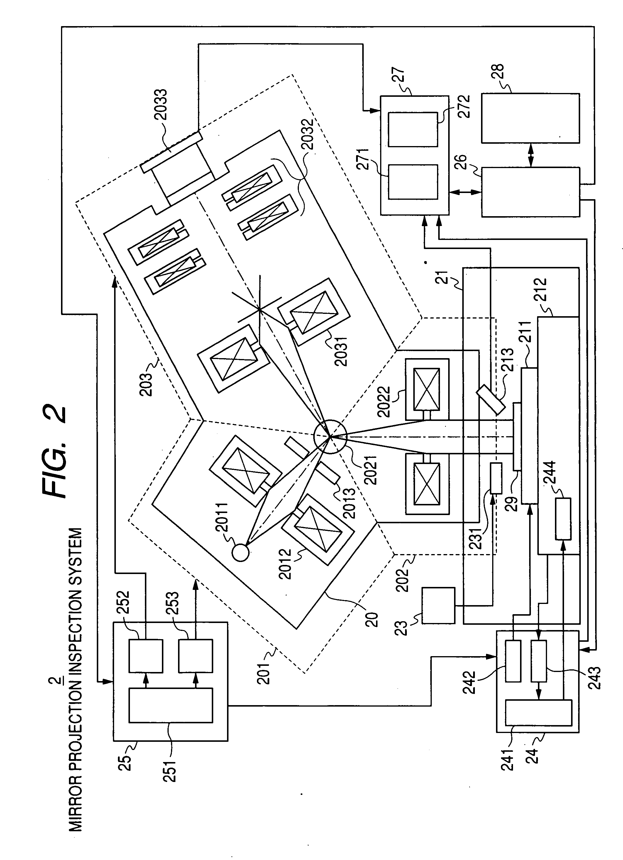
[0035]FIG. 2 schematically diagrams a mirror projection inspection system according to a first embodiment of the invention.
[0036]As shown in FIG. 2, a mirror projection inspection system 2 according to the embodiment includes: an electro-optic system 20; a sample chamber 21 where a sample (semiconductor wafer) 29 is placed; a charge control unit 23; a stage control unit 24; an electro-optic system control unit 25; a system control unit 26; an image processing unit 27; and a console terminal 28 for accepting an instruction from an operator or displaying information for an operator.
[0037]The electro-optic system 20 includes a radiation optics system 201, an imaging optics system 202, and a projection optics system 203. An evacuator (not shown) always places the electro-optic system 20 in an evacuated atmosphere.
[0038]The radiation optics system 201 includes a cathode 2011, a condenser lens 2012, and a diaphragm 2013. The imaging optics system 202 includes a beam separater 2021, and an...
second embodiment
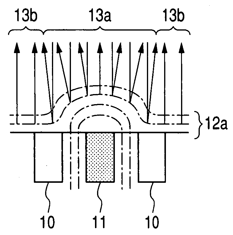
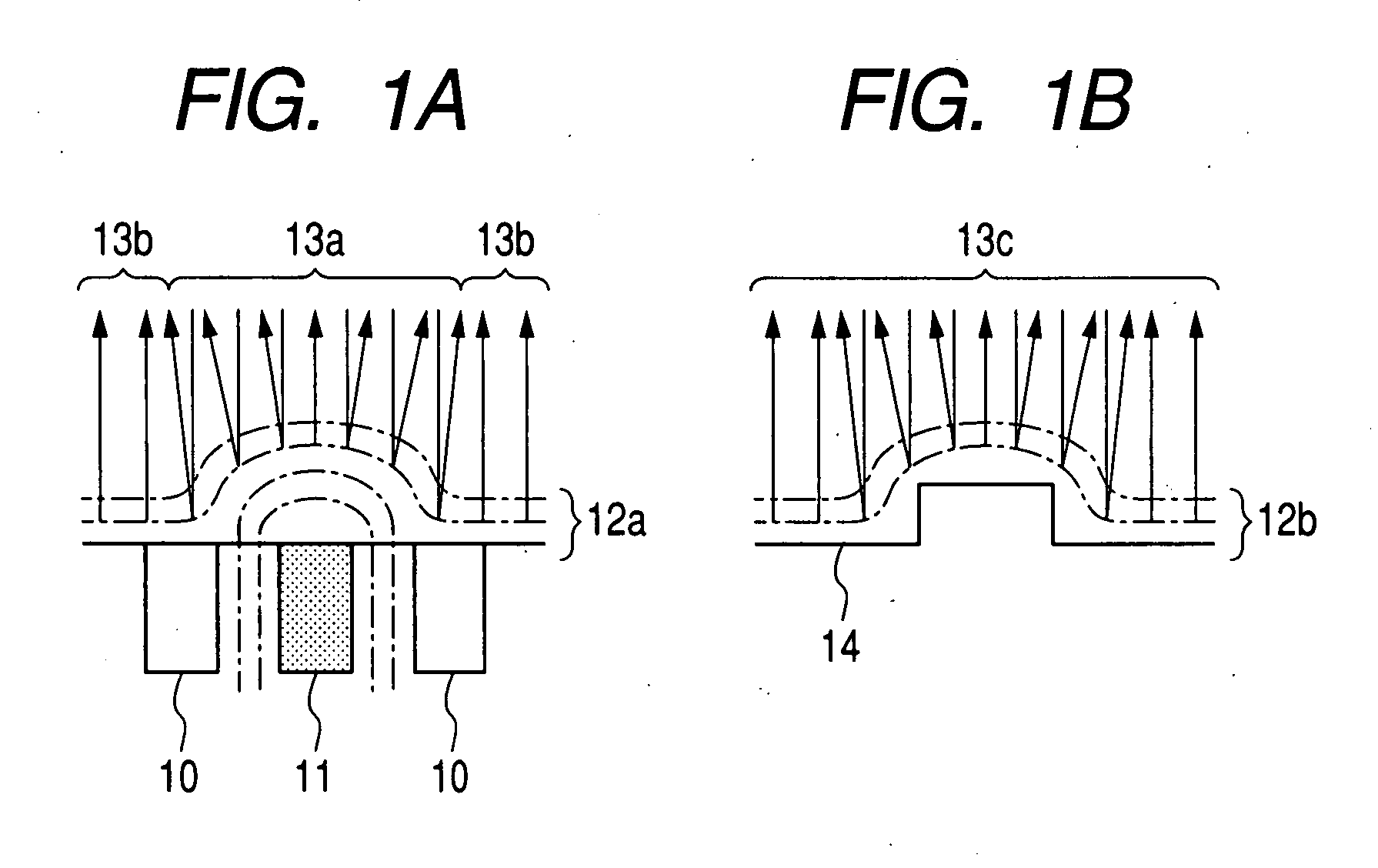
[0108]The second embodiment of the invention will be described. The second embodiment provides correction for the first embodiment so that a heightwise variation other than an elevation difference in the circuit pattern of the sample 29 (e.g., a macroscopic height variation due to the warpage of a semiconductor wafer) does not affect a height variation inspection result.
[0109]A mirror projection inspection system according to the second embodiment additionally provides the first embodiment shown in FIG. 2 with: a standard preparation for height correction mounted on the holder independently of the sample 29; and a height sensor for measuring heights of the sample 29 and the standard preparation for height correction mounted on the holder 211.
[0110]The height sensor can measure an average height of a region sized to several micrometers to several nanometers. This resolution is lower than a defective region the mirror projection inspection system can detect within a plane for the samp...
third embodiment
[0134]The third embodiment of the invention will be described. The embodiment allows the use of the AFM for measuring an elevation difference in the circuit pattern of the sample 29 in the first or second embodiment mentioned above.
[0135]FIG. 13 schematically shows a mirror projection inspection system according to a third embodiment of the invention. As shown in FIG. 13, the mirror projection inspection system according to the embodiment adds a sample chamber for AFM 31 to the first embodiment in FIG. 2 or the second embodiment.
[0136]A sample chamber 31 includes: an AFM 32; a holder 33 for mounting the sample 29; a stage 34 for moving the sample 29 perpendicularly to a needle of the AFM 32; an optical microscope for AFM 35; a transport unit (not shown) for transporting the sample 29 from the holder 211 to the holder 33; and a stage control unit (not shown) for controlling the stage 34. Unlike the sample chamber 21, the sample chamber 31 need not be evacuated. The inside of the samp...
PUM
 Abstract
Description
Claims
Application Information