Tile sub-array and related circuits and techniques

a technology of phased arrays and circuits, applied in the field of phased array antennas, can solve the problems of limiting the use of phased arrays in all but the most specialized applications, assembly and component costs, especially for active transmit/receive channels, are major cost drivers, etc., and achieve the effect of reducing the minimizing touch labor of components and assemblies, and high cost of phased arrays

Active Publication Date: 2008-03-27
RAYTHEON CO
View PDF19 Cites 297 Cited by
  • Summary
  • Abstract
  • Description
  • Claims
  • Application Information

AI Technical Summary

Benefits of technology

[0011]As mentioned above, the relatively high cost of phased arrays has precluded the use of phased arrays in all but the most specialized applications. Assembly and component costs, particularly for active transmit / receive channels, are major cost drivers. Phased array costs can be reduced by utilizing batch processing and minimizing touch labor of components and assemblies it would be advantageous to provide a tile sub-array for an Active, Electronically Scanned Array (AESA) that is compact, which can be manufactured in a cost-effective manner, that can be assembled using an automated process, and that can be individually tested prior to assembly into the AESA. There is also a need to lower acquisition and life cycle costs of phased arrays, while at the same time improving bandwidth, polarization diversity and robust RF performance characteristics to meet increasingly more challenging antenna performance requirements.
[0012]At least some embodiments of a tile sub-array architecture described herein enable a cost effective phased array solution for a wide variety of phased array radar missions or communication missions for ground, sea and airborne platforms. In addition, in at least one embodiment, the tile sub-array provides a thin, lightweight construction that can also be applied to conformal arrays on an aircraft wing or fuselage or on a Unmanned Aerial Vehicle (UAV).
[0013]In one so-called “packageless T / R channel” embodiment, a tile sub-array simultaneously addresses cost and performance for next generation radar and communication systems. Many phased array designs are optimized for a single mission or platform. In contrast, the flexibility of the tile sub-array architecture described herein enables a solution for a larger set of missions. For example, in one embodiment, a so-called upper multi-layer assembly (UMLA) and a lower multi-layer assembly (LMLA), each described further herein, serve as common building blocks. The UMLA is a layered RF transmission line assembly which performs RF signal distribution, impedance matching and generation of polarization diverse signals. Fabrication is based on multi-layer printed wiring board (PWB) materials and processes. The LMLA integrates a package-less Transmit / Receive (T / R) channel and an embedded circulator layer sub-assembly. In a preferred embodiment, the LMLA is bonded to the UMLA using a ball grid array (BGA) interconnect approach. The package-less T / R channel eliminates expensive T / R module package components and associated assembly costs. The key building block of the package-less LMLA is a lower multi-layer board (LMLB). The LMLB integrates RF, DC and Logic signal distribution and an embedded circulator layer. All T / R channel monolithic microwave integrated circuits (MMIC's) and components, RF, DC / Logic connectors and thermal spreader interface plate can be assembled onto the LMLA using pick and place equipment.
[0015]With this particular arrangement, a tile sub-array can be manufactured without the need to perform any back-drill and back-fill operations typically required to eliminate RF via stubs. The RF matching pad technique refers to a technique in which a conductor is provided on blank layers (i.e., layers with no copper) of a circuit board or in ground plane layers (with etched relief area) of a circuit board. The conductor and associated relief area provided the mechanism to adjust impedance characteristics of RF vias (also referred to as RF interconnect circuits) provided in a circuit board. Since the need to utilize back-drill and back-fill operations is eliminated, the RF matching pad approach enables a standard, low aspect ratio drill and plate manufacturing operation to produce an RF via that connects inner circuit layers and which also has a low insertion loss characteristic across a desired frequency band such as X-Band (8 GHz-12 GHz).
[0016]As is known, mode suppression vias help electrically isolate the RF interconnects from surrounding circuitry, thereby preventing signals from “leaking” between signal paths. In conventional systems, the mode suppression vias are also drilled and plated at the same time the interconnecting RF via is drilled and plated.
[0017]With the RF matching pad approach of the present invention, however, all RF and mode suppression vias can be drilled and plated through the entire assembly and there is no need to utilize and back drill and fill operations on the RF interconnects. Thus, manufacturing costs associated with back drill and back fill operations can be completely eliminated while simultaneously improving RF performance because channel to channel variations due to drill tolerances and backfill material tolerances are eliminated.

Problems solved by technology

As mentioned above, the relatively high cost of phased arrays has precluded the use of phased arrays in all but the most specialized applications.
Assembly and component costs, particularly for active transmit / receive channels, are major cost drivers.

Method used


Image

  • Tile sub-array and related circuits and techniques
  • Tile sub-array and related circuits and techniques
  • Tile sub-array and related circuits and techniques

Examples


Embodiment Construction

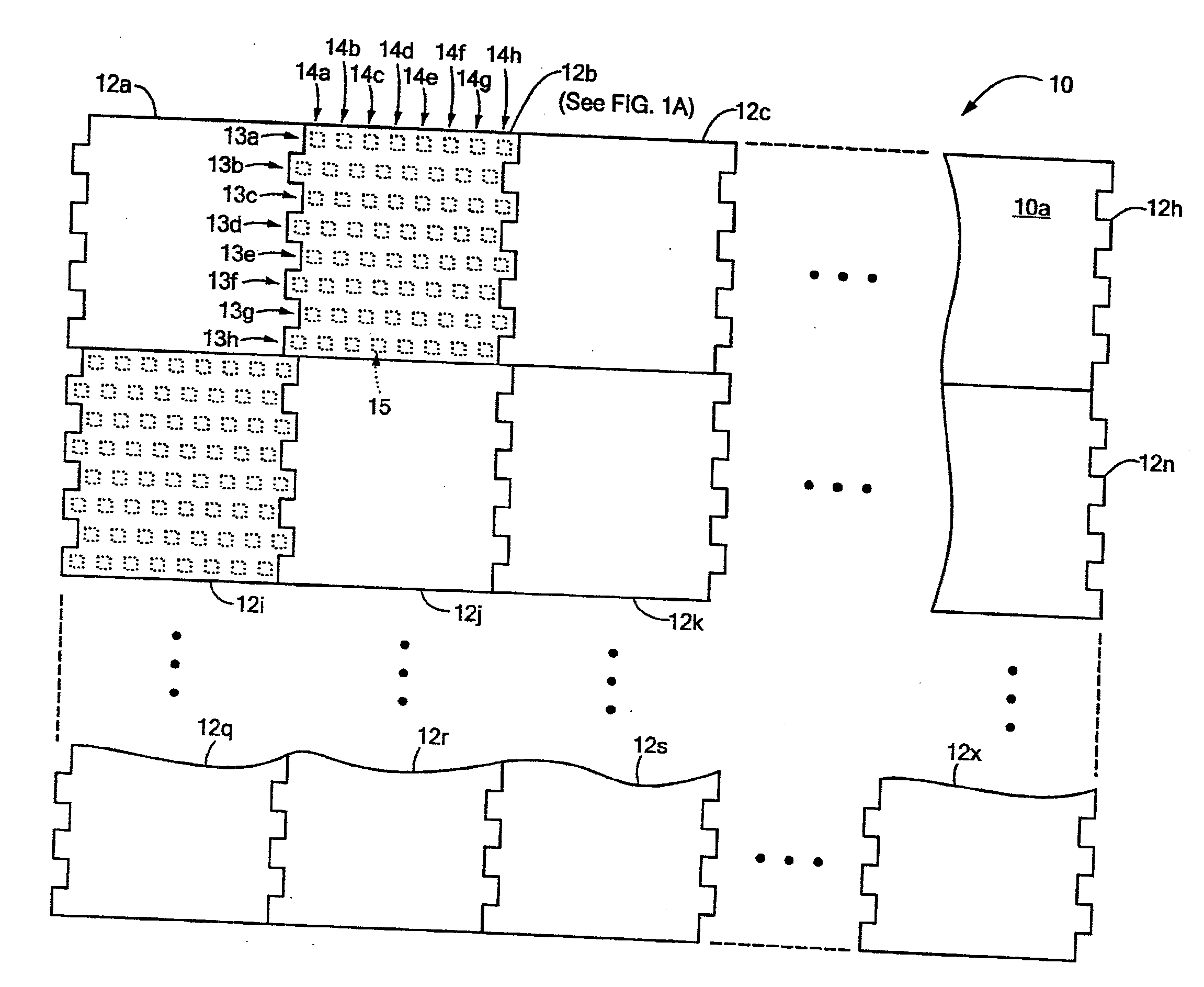
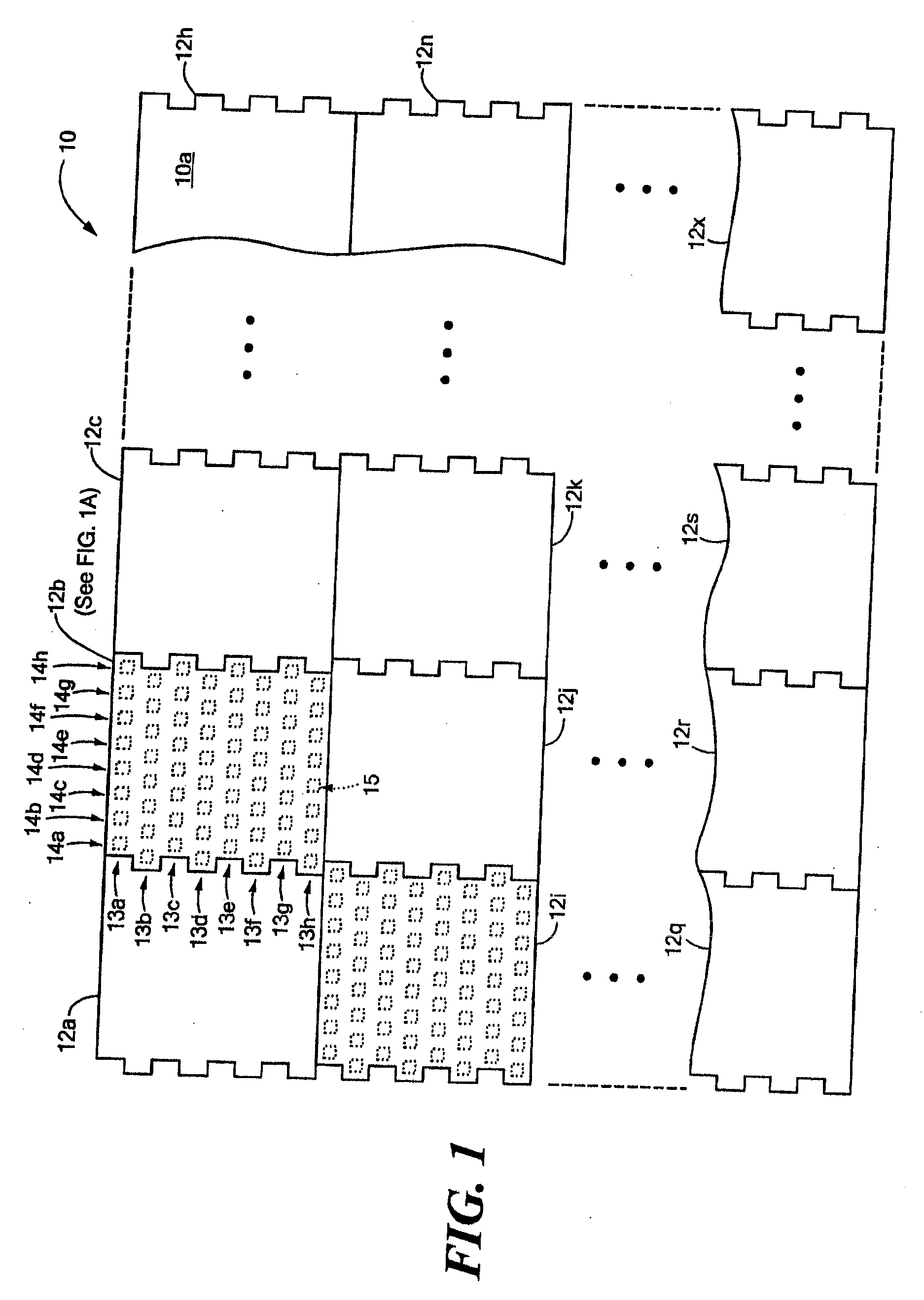
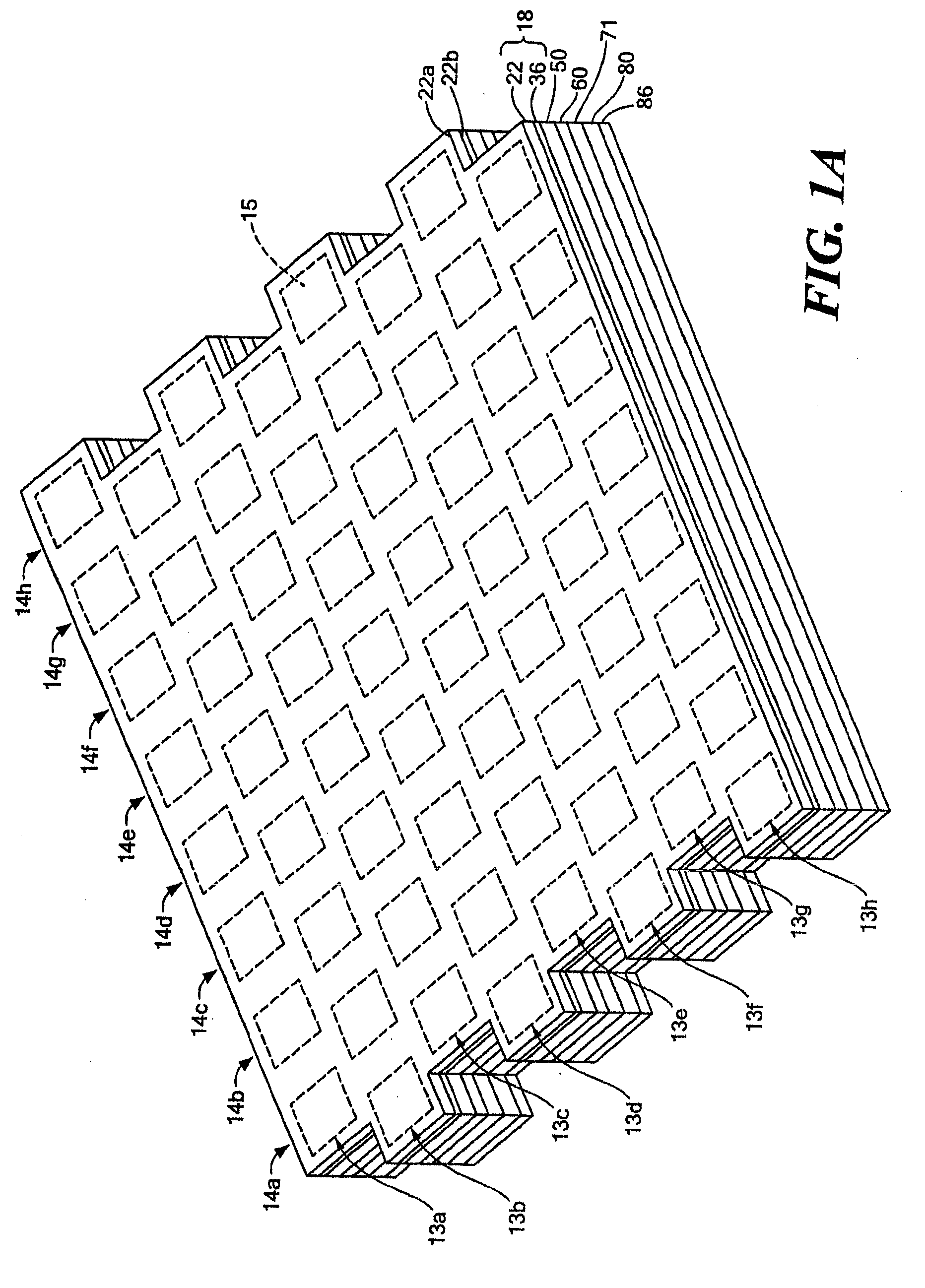
[0040]Before describing the various embodiments of the invention, it should be noted that reference is sometimes made herein to an array antenna having a particular array shape and / or size (e.g., a particular number of antenna elements or a particular number of tiles) or to an array antenna comprised of a particular number of “tile sub-arrays” (or more simply “tiles”). One of ordinary skill in the art will appreciate that the techniques described herein are applicable to various sizes and shapes of array antennas.

[0041]Similarly, reference is sometimes made herein to tile sub-arrays having a particular geometric shape (e.g. square, rectangular, round) and / or size (e.g., a particular number of antenna elements) or a particular lattice type or spacing of antenna elements. One of ordinary skill in the art will appreciate that the techniques described herein are applicable to various sizes and shapes of array antennas as well as to various sizes and shapes of tile sub-arrays.

[0042]Thus,...


PUM


Abstract

A radiator includes a waveguide having an aperture and a patch antenna disposed in the aperture. In one embodiment, an antenna includes an array of waveguide antenna elements, each element having a cavity, and an array of patch antenna elements including an upper patch element and a lower patch element disposed in the cavity.

Description

FIELD OF THE INVENTION[0001]This invention relates generally to phased array antennas adapted for volume production at a relatively low cost and having a relatively low profile and more particularly to radio frequency (RF) circuits and techniques utilized in phased array antennas.BACKGROUND OF THE INVENTION[0002]As is known in the art, a phased array antenna includes a plurality of antenna elements spaced apart from each other by known distances coupled through a plurality of phase shifter circuits to either or both of a transmitter or receiver. In some cases, the phase shifter circuits are considered to be part of the transmitter and / or receiver.[0003]As is also known, phased array antenna systems are adapted to produce a beam of radio frequency energy (RF) and direct such beam along a selected direction by controlling the phase (via the phase shifter circuitry) of the RF energy passing between the transmitter or receiver and the array of antenna elements. In an electronically scan...

Claims


Application Information

Patent Timeline
Patent Type & Authority Applications(United States)
IPC IPC(8): H01Q1/38G06Q30/00
CPCH01Q21/22H01Q21/0025
Inventor PUZELLA, ANGELO M.CROWDER, JOSEPH M.DUPUIS, PATRICIA S.FALLICA, MICHAEL C.FRANCIS, JOHN B.LICCIARDELLO, JOSEPH A.
Owner RAYTHEON CO
Why Eureka
Try Eureka