Method of uniform phosphor chip coating and led package fabricated using method

a technology of phosphor chip and led package, which is applied in the manufacture of semiconductor/solid-state devices, semiconductor devices, electrical equipment, etc., can solve the problems of non-uniform white light emitted by led package, complex and costly method for achieving uniform phosphor coating directly on led package, and the dominance of sideways light emitted into high viewing angl

Active Publication Date: 2008-04-03
CREELED INC
View PDF67 Cites 72 Cited by
  • Summary
  • Abstract
  • Description
  • Claims
  • Application Information

AI Technical Summary

Problems solved by technology

This packaging, however, can result in an LED package having significant variation of the color and hue of emitted light at different viewing angles with respect to the package.
This problem can be made worse in packages where the phosphor containing matrix material extends above the “rim” of the cup in which the LED resides, resulting in a predominance of converted light emitted sideways into high viewing angles (e.g. at 90 degrees from the optic axis).
The result is that the white light emitted by the LED package becomes non-uniform and can have bands or patches of light having different colors or intensities.
This, however, is typically a complex and costly method for achieving uniform phosphor coating directly on an LED.
The method can be slow, messy and can present inconsistencies due to difficulties in controlling electrostatic charges across many LEDs in a mass production environment.
This can put stresses on the components through the operating temperature cycle of the LED package that can result in reliability issues such as delamination of encapsulant from reflector or substrate walls, cohesive fracture within the encapsulant itself, and damage to LED chip wire bonds.

Method used


Image

  • Method of uniform phosphor chip coating and led package fabricated using method
  • Method of uniform phosphor chip coating and led package fabricated using method
  • Method of uniform phosphor chip coating and led package fabricated using method

Examples


Embodiment Construction

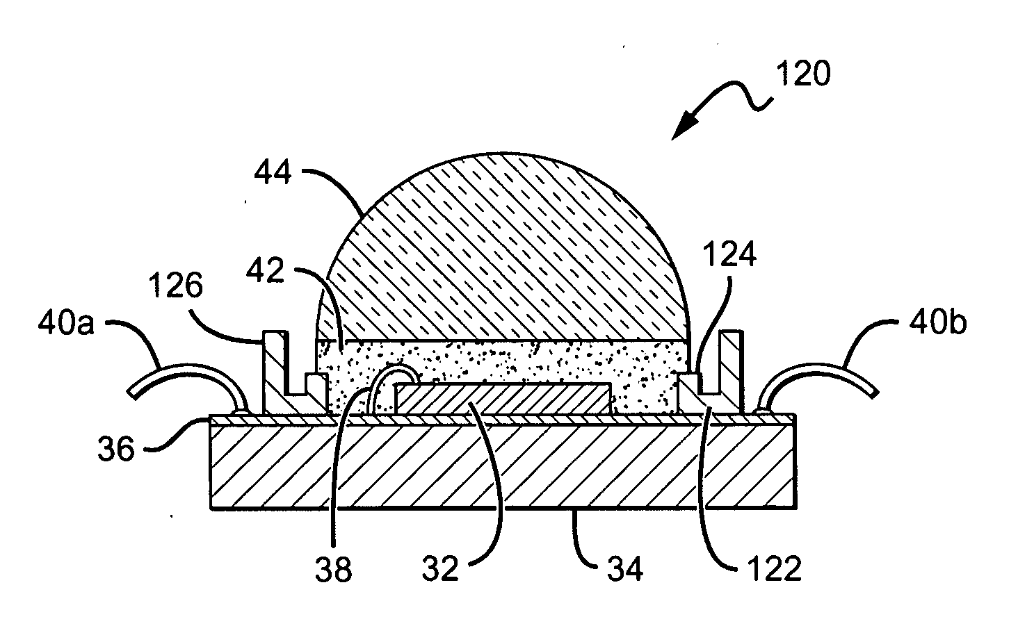
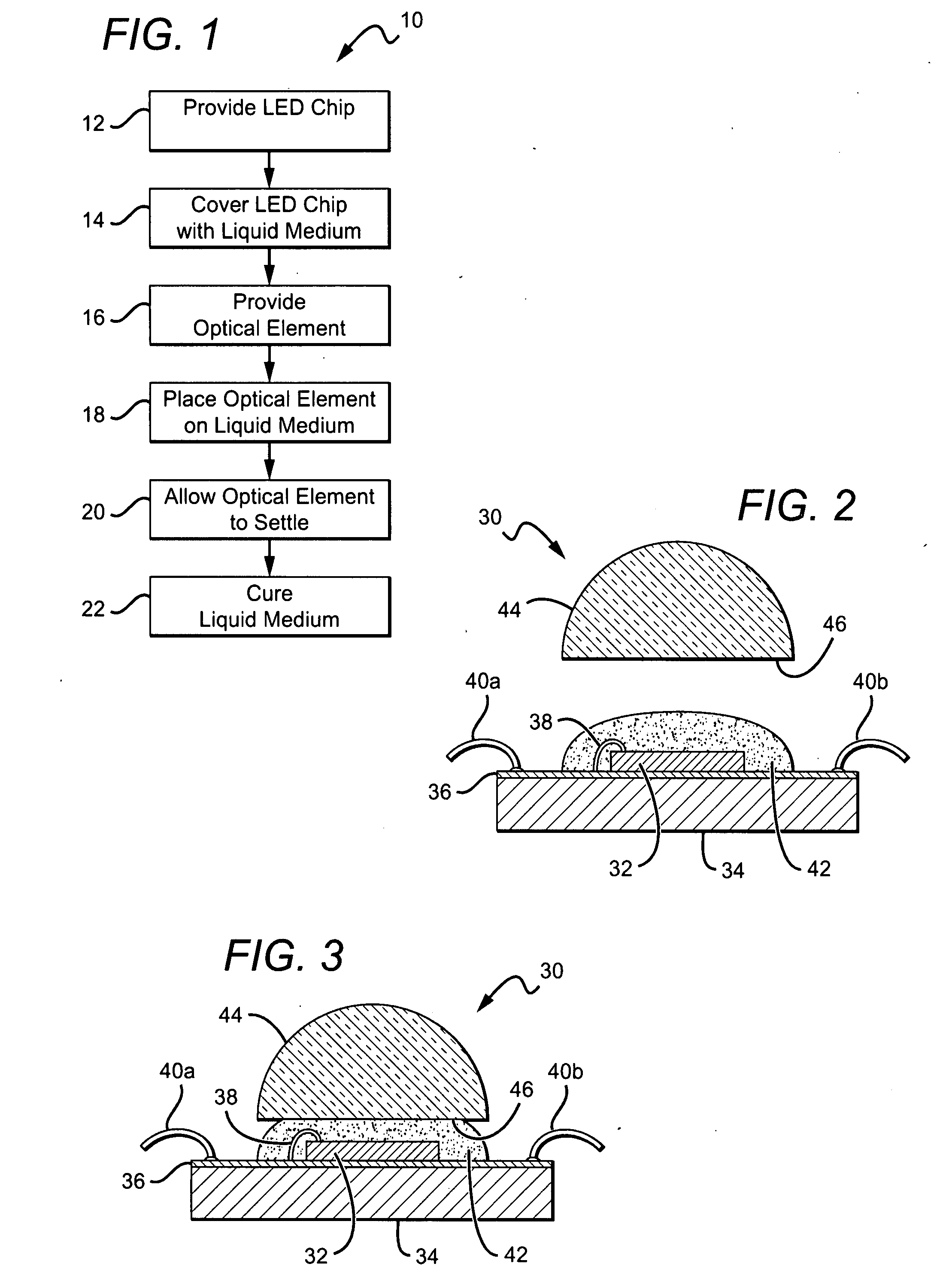
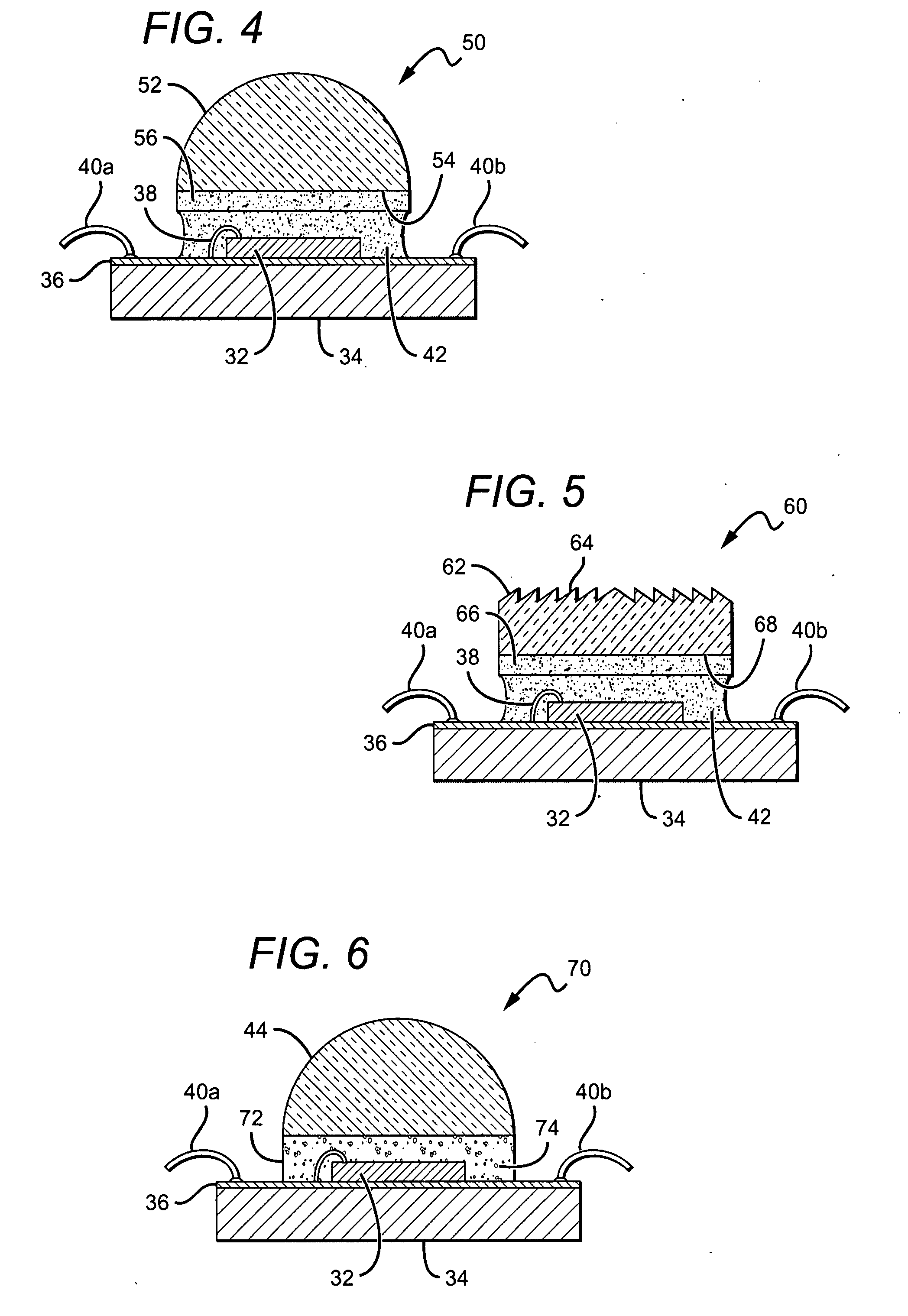
[0023] The present invention relates to methods for fabricating semiconductor chip packages, and in particular LED chip packages having substantially uniform phosphor coatings over their LED chips. The invention also relates to LED packages fabricated using the methods. In one method, a liquid is deposited over an LED chip and an optical element is placed on top of the liquid medium and allowed to settle on the liquid medium at the desired level. In one embodiment, the term settle refers to an equilibrium point reached between the lens and liquid medium where the lens stops moving down under the force of gravity. In other embodiments, the lens does not need to reach an equilibrium point, but instead, the liquid medium can be cured prior to the lens and liquid reaching an equilibrium.

[0024] The top surface of the liquid medium takes the shape of the bottom surface of the optical element, and the level of which the optical element settles is determined by a number of factors as descr...


PUM


Abstract

Methods for fabricating LED packages comprising providing an LED chip and covering at least part of it with a liquid medium. An optical element is provided and placed on the liquid medium. The optical element is allowed to settle to a desired level and the liquid medium is cured. LED packages are also disclosed that are fabricated using the disclosed methods.

Description

BACKGROUND OF THE INVENTION [0001] 1. Field of the Invention [0002] This invention relates to light emitting diodes (LED or LEDs) and more particularly to methods for coating LEDs with a conversion material and LED packages fabricated using the methods. [0003] 2. Description of the Related Art [0004] Light emitting diodes (LEDs) are solid state devices that convert electric energy to light, and generally comprise one or more active layers of semiconductor material sandwiched between oppositely doped layers. When a bias is applied across the doped layers, holes and electrons are injected into the active layer where they recombine to generate light. Light is emitted from the active layer and from all surfaces of the LED. [0005] Conventional LEDs cannot generate white light from their active layers. One way to produce white light from conventional LEDs is to combine different colors from different LEDs. For example, the light from red, green and blue LEDs, or blue and yellow LEDs can b...

Claims


Application Information

Patent Timeline
Patent Type & Authority Applications(United States)
IPC IPC(8): H01L33/00H01L33/50H01L33/52H01L33/58
CPCH01L33/505H01L33/54H01L33/58H01L2933/0041H01L2933/005H01L2924/19107H01L2224/48091H01L2924/00014
Inventor LOH, BAN P.MEDENDORP, NICHOLAS W. JR.ANDREWS, PETERFU, YANKUNLAUGHNER, MICHEALLETOQUIN, RONAN
Owner CREELED INC
Why Eureka
Try Eureka