Electronic device and method of manufacturing the same

a technology of electronic devices and manufacturing methods, applied in the direction of printed circuit manufacturing, printed circuit aspects, lamination of printed circuit boards, etc., can solve the problems of reducing the cost of electronic devices, restricting the resin which is lower in decomposition temperature than the resin, etc., and achieves the effect of low cost and low cos

Active Publication Date: 2008-04-03
RENESAS ELECTRONICS CORP
View PDF6 Cites 67 Cited by
  • Summary
  • Abstract
  • Description
  • Claims
  • Application Information

AI Technical Summary

Benefits of technology

[0010]There is provided a method of manufacturing an electronic device, including: wherein in the step of said forming second interconnect layer, a resin which is lower is in decomposition temperature than a resin which constitutes said first interconnect layer is used as a resin which constitutes said second interconnect layer. Therefore, resin suitable for micromachining can be used in the first interconnect layer; on the other hand, resin with relatively low cost can be used in the second interconnect layer.
[0012]In this electronic device, as a resin which constitutes the second interconnect layer, resin which is lower in decomposition temperature than resin which constitutes the first interconnect layer can be used. Therefore, resin suitable for micromachining can be used in the first interconnect layer; on the other hand, resin with relatively low cost can be used in the second interconnect layer.
[0013]According to the present invention, there can be implemented an electronic device and a method of manufacturing the same, both of which are capable of obtaining microscopic connection between an interconnect layer and an electronic component with low cost.

Problems solved by technology

As a result, there is a restriction in that resin which is lower in decomposition temperature than the resin which constitutes the interconnect layer on the electronic component side cannot be used as the resin which constitutes the interconnect layer on the solder ball side.
The resin for use in the interconnect layer on the solder ball side is limited for such a restriction, and accordingly, reduction in cost of the electronic device is hindered.

Method used


Image

  • Electronic device and method of manufacturing the same
  • Electronic device and method of manufacturing the same
  • Electronic device and method of manufacturing the same

Examples


first embodiment

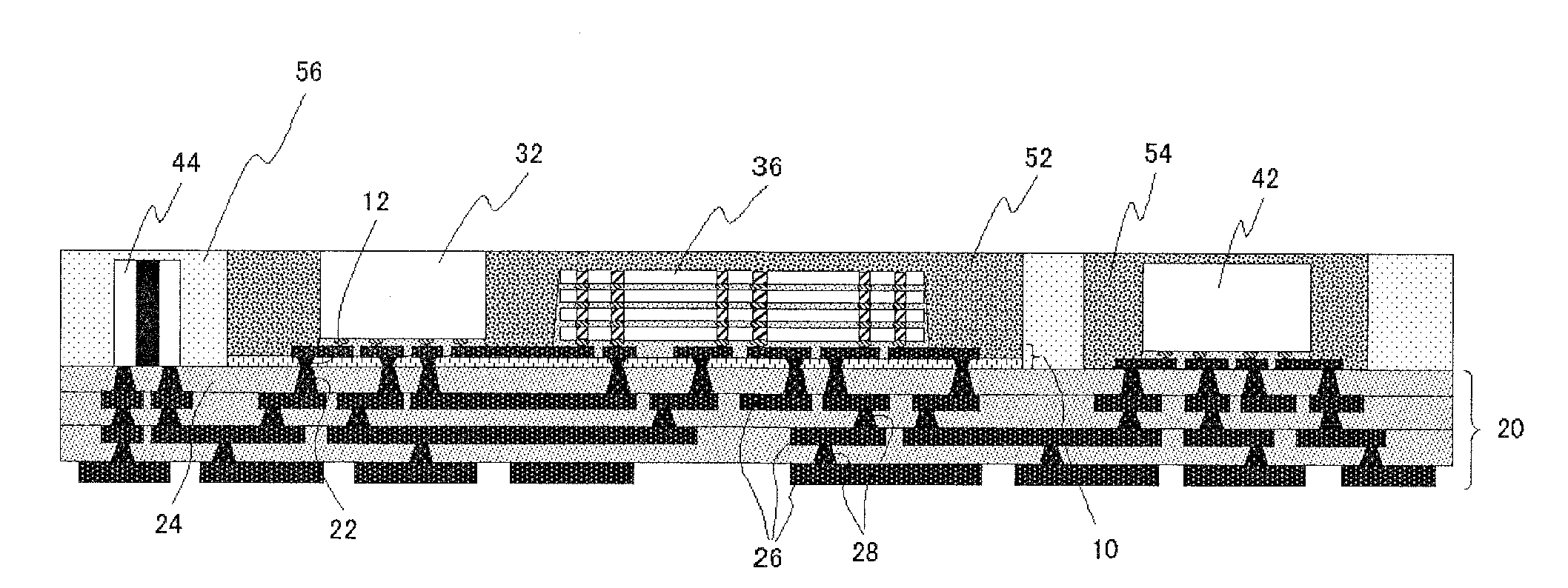
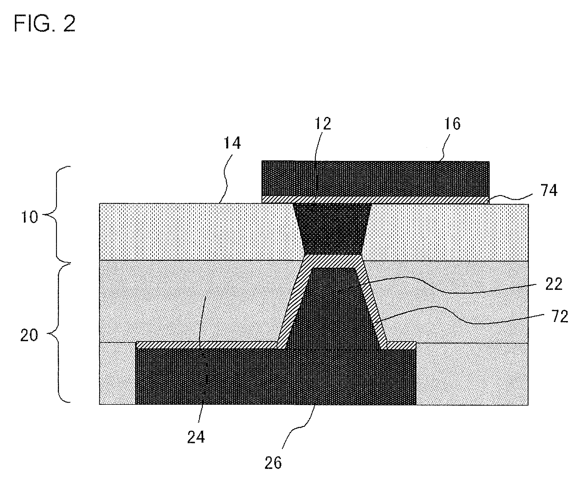
[0033]FIG. 1 is a cross-sectional view showing a first embodiment of an electronic device according to the present invention. An electronic device 1 includes an interconnect layer 10 (a first interconnect layer) and an interconnect layer 20 (a second interconnect layer).

[0034]The interconnect layer 10 has a via plug 12 (a first conductive plug), an insulation resin 14, and conductor interconnect 16. The via plug 12 is formed in the insulation resin 14. As can be seen from the drawing, the via plug 12 is of a tapered shape which becomes smaller in diameter as approaching to the interconnect layer 20. Therefore, an end surface area on the interconnect layer 20 side of the via plug 12 is smaller than an end surface area opposite thereto, that is, an end surface area on the IC chip 32 and 36 sides (to be described later).

[0035]A conductor of the via plug 12 is Cu, Ni, Au, or Ag, for example. The insulation resin 14 is, for example, polyimide resin, polybenzoxazole (referred to as PBO) r...

second embodiment

[0063]FIG. 8 is a cross-sectional view showing a second embodiment of an electronic device according to the present invention. The electronic device 2 includes an interconnect layer 10 (a first interconnect layer) and interconnect layer 80 (a second interconnect layer). Configuration of the interconnect layer 10 is the same as that described in FIG. 1.

[0064]The interconnect layer 80 is formed on an undersurface of the interconnect layer 10 and extended to further outside than the interconnect layer 10. The interconnect layer 80 has a solder resist 84 and conductor interconnect 86 formed therein. Resin which is lower in decomposition temperature than an insulation resin 14 is used as the solder resist 84. A via plug 82 (a second conductive plug) is formed in the interconnect layer 80. The via plug 82 corresponds to a portion buried in a part of a solder ball 60, specifically in the solder resist 84 in the solder ball 60. As can be seen from the drawing, the via plug 82 is of a tapere...

third embodiment

[0071]FIG. 13 is a cross-sectional view showing a third embodiment of an electronic device according to the present invention. The electronic device 3 includes an interconnect layer 10 and an interconnect layer 80. The electronic device 3 is different from the electronic device 2 shown in FIG. 8 in that the interconnect layer 80 has a multilayer interconnect structure. In the present embodiment, the interconnect layer 80 includes an insulation resin 84a provided on an undersurface of the interconnect layer 10 and a solder resist 84b provided thereon.

[0072]In the interconnect layer 80 of the present embodiment, conductor interconnect 86 provided in plural layers and a via plug 83 (a second conductive plug) connected to the conductor interconnect 86 are formed. As can be seen from the drawing, the via plug 83 is of a tapered shape which becomes smaller in diameter as approaching to the interconnect layer 10. Therefore, an end surface area on the interconnect layer 10 side of the via p...


PUM


Abstract

In a conventional electronic device and a method of manufacturing the same, reduction in cost of the electronic device is hindered because resin used in an interconnect layer on the solder ball side is limited. The electronic device includes an interconnect layer (a first interconnect layer) and an interconnect layer (a second interconnect layer). The second interconnect layer is formed on the undersurface of the first interconnect layer. The second interconnect layer is larger in area seen from the top than the first interconnect layer and is extended to the outside from the first interconnect layer.

Description

[0001]This application is based on Japanese patent application No. 2006-271154, the content of which is incorporated hereinto by reference.BACKGROUND[0002]1. Technical Field[0003]The present invention relates to an electronic device and a method of manufacturing the same.[0004]2. Related Art[0005]As a known method of manufacturing an electronic device, for example, there is provided one which is disclosed in Japanese Laid-open patent publication No. 2003-309215. In a manufacturing method described in the same document, a multilayer interconnect layer is formed by laminating a plurality of interconnect layers on a supporting substrate, and then, the supporting substrate is removed. Then, a solder ball is formed as an external electrode terminal on one surface of the multilayer interconnect layer which is exposed by the removal of the supporting substrate. Furthermore, electronic components are mounted in a flip chip configuration on the other surface of the multilayer interconnect la...

Claims


Application Information

Patent Timeline
Patent Type & Authority Applications(United States)
IPC IPC(8): H01L23/52H01L21/4763
CPCH01L21/6835H01L2224/16235H01L23/3121H01L24/16H01L25/0652H01L25/16H01L2221/68345H01L2224/16H01L2924/01079H01L2924/09701H01L2924/14H01L2924/15311H01L2924/1532H01L2924/19015H01L2924/19041H01L2924/19105H05K3/0058H05K3/284H05K3/4682H05K2201/0195H05K2201/09527H05K2201/096H05K2201/09972H05K2203/016H05K2203/0733H05K2203/1469H01L23/5384H01L23/5226H01L23/49816H01L2224/16145H01L2224/16225H01L2224/81005H01L2924/15192H01L2924/18161H01L23/13H01L2224/83005H01L21/568H01L2224/16146H01L2224/16238H01L2224/17181H01L2224/32145H01L2224/32225H01L2224/73204H01L2924/12042H01L2924/00014H01L2924/00011H01L2924/00H01L2224/0401H01L23/522H01L25/0657H01L25/50H01L2225/06513H01L2225/06544H01L2225/06555H01L2225/06582H01L23/5383H01L23/5386H01L24/02H01L25/18H01L2221/68372H01L2224/02319H01L2224/02331H01L2224/02333H01L2224/02372H01L2224/02373H01L2224/02379H01L2224/02381H01L2224/16137
Inventor KURITA, YOICHIROKAWANO, MASAYASOEJIMA, KOJI
Owner RENESAS ELECTRONICS CORP
Why Eureka
Try Eureka