
Electronic device and metal plate member

a metal plate and electronic technology, applied in the direction of electrical apparatus construction details, electrical apparatus casings/cabinets/drawers, instruments, etc., can solve problems such as becoming difficult, and achieve the effect of reducing radio wave noise effectively and better utilizing a narrow spa

Inactive Publication Date: 2008-04-03
FUJITSU CLIENT COMPUTING LTD
View PDF13 Cites 15 Cited by
  • Summary
  • Abstract
  • Description
  • Claims
  • Application Information

AI Technical Summary

Benefits of technology

[0016]In a typical notebook PC or pure-tablet PC, two connectors are placed on the main board which is the first substrate, so as to incorporate the sub substrate which is the second substrate such as a memory board for increasing memory capacity.
[0017]The electronic device according to the invention utilizes a dead space between the two connectors by placing the metal plate member in the space and fastening the metal plate member to the metal housing. This allows better use of a narrow space as well as suppression of radio wave noise by electrically connecting the ground of the first substrate to the metal housing.
[0020]Here, it is preferable that the second substrate is typically a memory board mounted with a memory. More preferably, the housing is made of a magnesium alloy for making the device thinner and lighter while maintaining strength.
[0024]As described above, the electronic device according to the present invention is capable of reducing radio wave noise effectively by better utilizing a narrow space.

Problems solved by technology

Additionally, a cable or the like used for connection to another device compromises the mobility of such mobile PCs, so that many mobile PCs incorporate radio communication features conforming to various standards, such as the wireless LAN and the Bluetooth (registered trademark).
Meanwhile, conventional measures against noise have needed certain space in a device for suppressing noise, which is becoming difficult due to the latest demand for a thinner and lighter device.

Method used


Image

  • Electronic device and metal plate member
  • Electronic device and metal plate member
  • Electronic device and metal plate member

Examples


Embodiment Construction

[0053]In the following, an embodiment of the present invention will be described.

[0054][Overall Configuration]

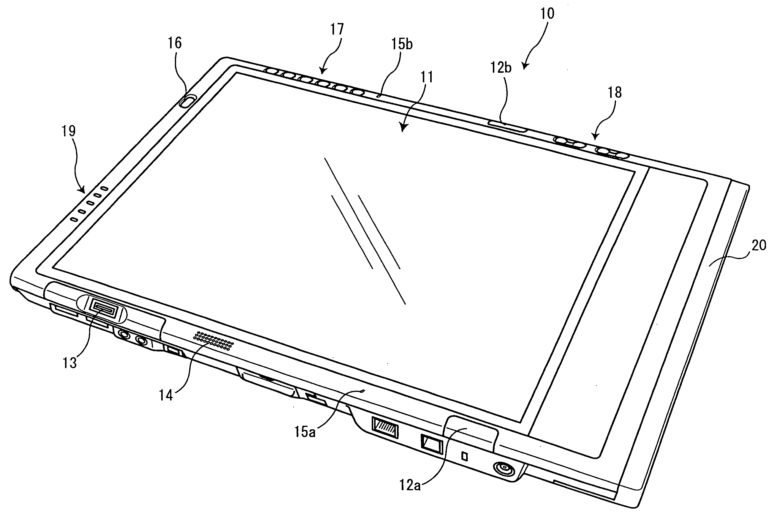
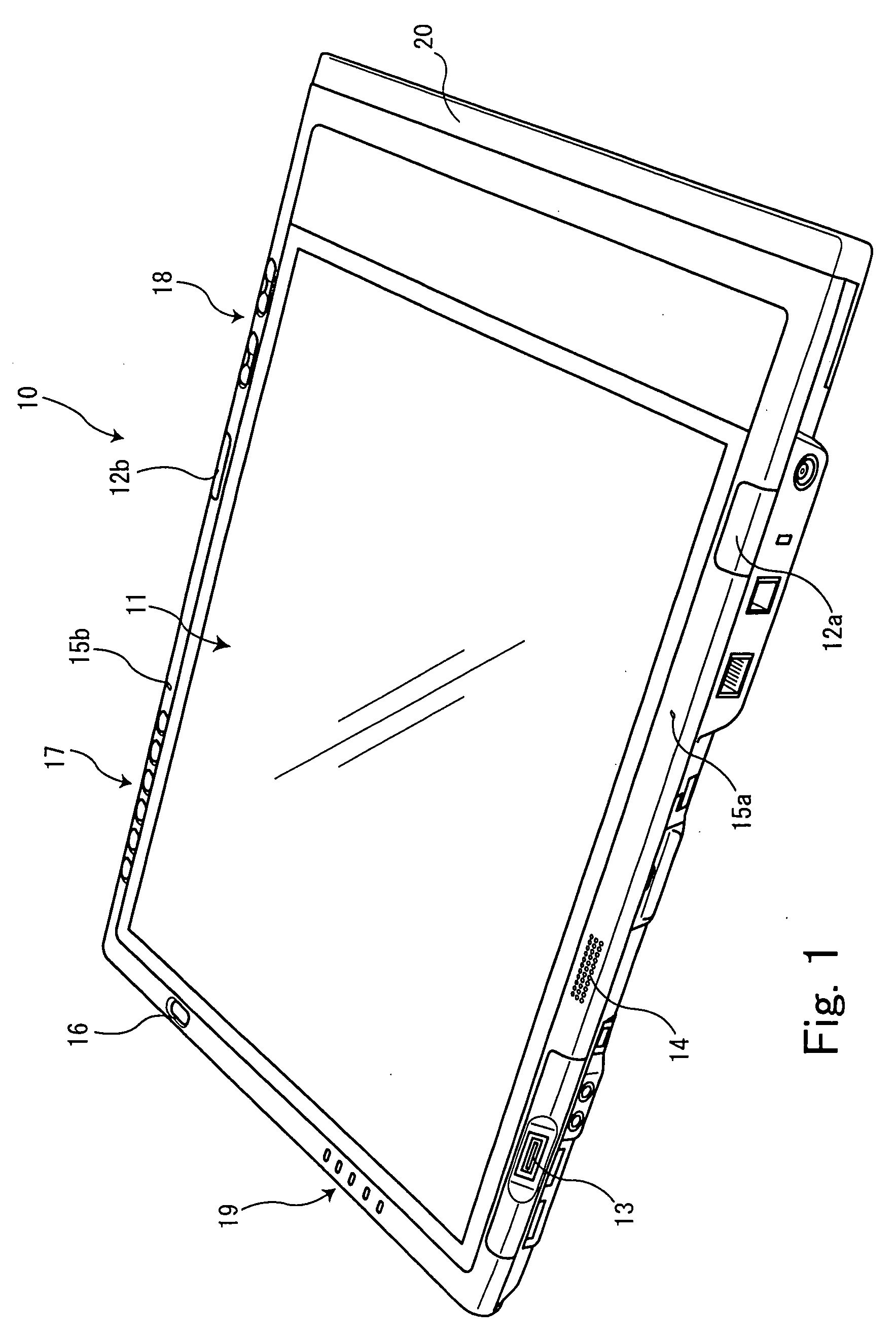
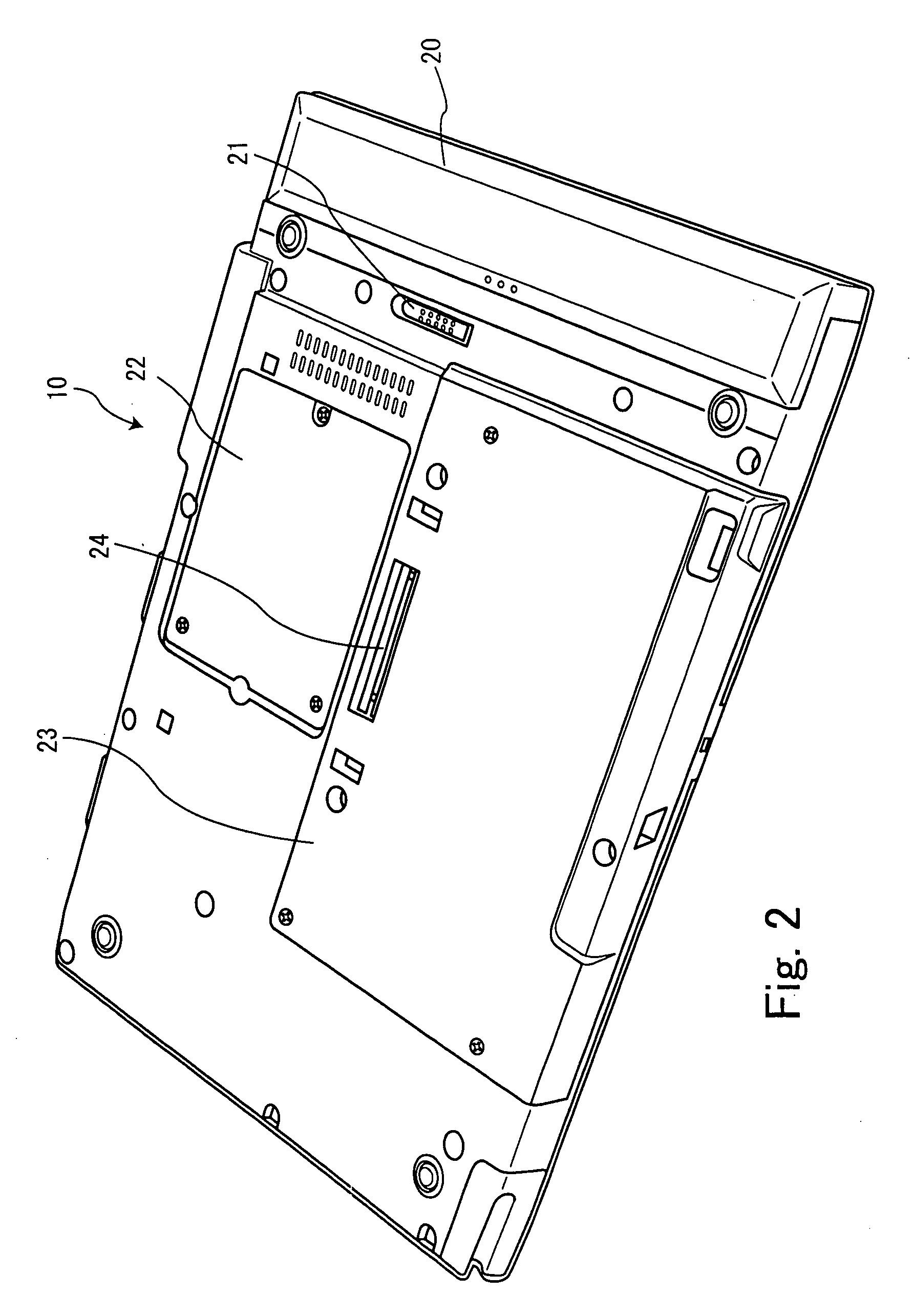
[0055]FIG. 1 is a perspective view of a slate PC, which is an electronic device according to an embodiment of the present invention, seen from the top surface having a display screen formed thereon. FIG. 2 is a perspective view of the slate PC shown in FIG. 1 seen from the bottom surface.

[0056]A slate PC 10 has a housing made of a magnesium alloy that forms the bottom surface and the side surfaces of the slate PC 10 and an image display panel that has a display screen for displaying images and covers the front of the housing with the display screen facing outwardly. The housing and the image display panel form the exterior of the slate PC 10.

[0057]On the front surface of the slate PC 10, the image display panel is disposed with a display screen 11 facing outwardly. Two infrared communication windows 12a and 12b and a fingerprint sensor 13 are arranged around the image displa...


PUM


Abstract

An electronic device includes: a metal housing with an opening; a metal lid that is attached to the housing so as to cover the opening; a first substrate fixed in the housing and spread facing and parallel to the opening; two connectors that are fixed in the housing at a position facing and closer to the opening than the first substrate and are spread facing and parallel to the opening, the two connectors extending parallel to each other such that there is a predetermined space between the two connectors, the two connectors each being capable of receiving a second substrate that is inserted therein toward the space; and a metal plate member disposed in the space so that the metal plate member is fastened to the housing and resiliently contacts a surface of the first substrate, thereby electrically connecting a ground of the first substrate to the housing.

Description

BACKGROUND OF THE INVENTION[0001]1. Field of the Invention[0002]The present invention relates to an electronic device that has a substrate mounted with an electronic circuit and accommodated in a housing and to a metal plate member employed in the electronic device.[0003]2. Description of the Related Art[0004]Recently, various types of mobile personal computers (abbreviated as PC hereinafter) have come into widespread use. One such a PC is a so-called notebook PC composed of a main unit incorporating an arithmetic circuit and having a keyboard on the front surface thereof and a display unit having a display screen and being capable of folded onto the main unit. Another type of such a PC is a pure-tablet (slate) PC that incorporates an arithmetic circuit and has a display screen on the top surface thereof, to which a keyboard is optionally externally connected.[0005]Such mobile PCs are made thinner to reduce the overall size and weight while maintaining the required display screen si...

Claims


Application Information

Patent Timeline
IPC IPC(8): H05K5/04
CPCG06F1/1626G06F1/1635G06F1/1656G06F1/1658H05K9/0049G06F1/182G06F1/185G06F1/203G06F1/1684
Inventor CHIKAZAWA, NAGAHISAADACHI, KATSUMI
Owner FUJITSU CLIENT COMPUTING LTD
Learn More