Semiconductor device and manufacturing method thereof

a technology of semiconductor devices and manufacturing methods, applied in the direction of semiconductor devices, basic electric elements, electrical appliances, etc., can solve the problems of inability to obtain satisfaction in terms of cost, manufacturing time and the like, and long filling time, etc., to achieve the effect of reducing the overflow of sealing resin, good sealing quality and low cos

Inactive Publication Date: 2008-04-03
LAPIS SEMICON CO LTD
View PDF5 Cites 14 Cited by
  • Summary
  • Abstract
  • Description
  • Claims
  • Application Information

AI Technical Summary

Benefits of technology

[0008]With the foregoing in view, it is therefore an object of the present invention to provide a method for manufacturing a semiconductor device, which is capable of suppressing an overflow of a sealing resin and obtaining good sealing quality, simply and at low cost. It is another object of the present invention to provide a semiconductor device which suppresses an overflow of a sealing resin and has good sealing quality, simply and at low cost.
[0010]According to a second aspect of the present invention, there is provided a method wherein the viscosity of the first sealing resin is higher than that of the second sealing resin.

Problems solved by technology

However, a problem arises in that when the difference between the outer shape of the semiconductor chip and the outer shape of the mounting board is made small, the sealing resin covers external terminals provided around a chip mounting area of the mounting board due to an overflow of the sealing resin, thereby causing a poor connection.
Although a reduction in its overflow can be improved by adaptation of a high-viscosity sealing resin, its filling needs a long period of time and voids and unfilling are easy to occur.
However, the present situation is that the above proposal adopts a technique for applying the resin over the entire surface of the mounting board for dam formation and thereafter processing it into a predetermined shape in accordance with a photolitho process and cannot obtain satisfaction in terms of cost, manufacturing time and the like.

Method used


Image

  • Semiconductor device and manufacturing method thereof
  • Semiconductor device and manufacturing method thereof
  • Semiconductor device and manufacturing method thereof

Examples


first preferred embodiment

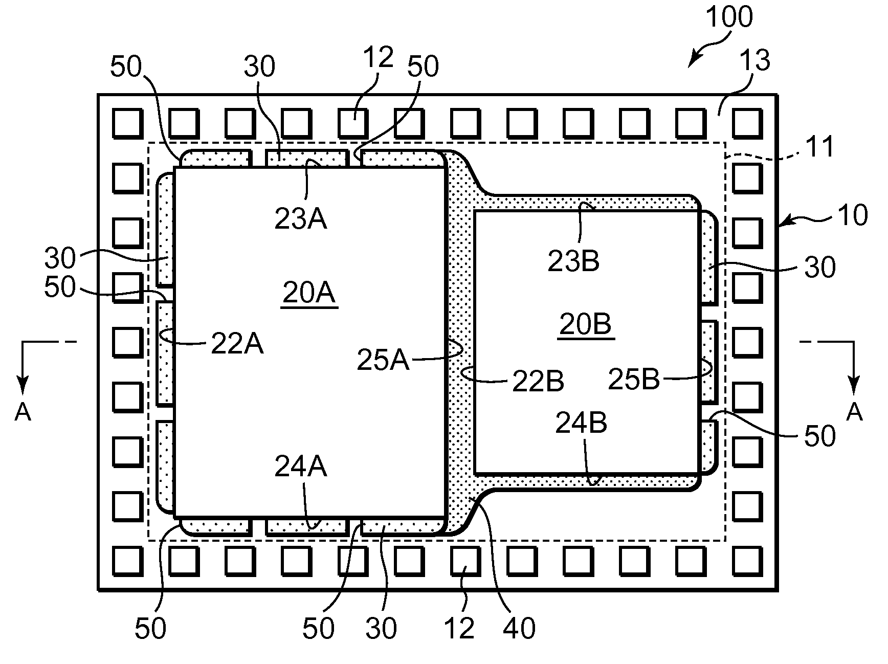
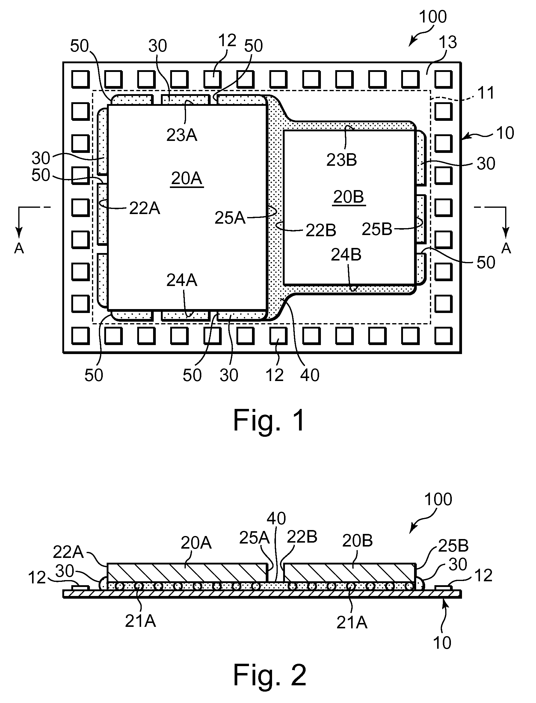
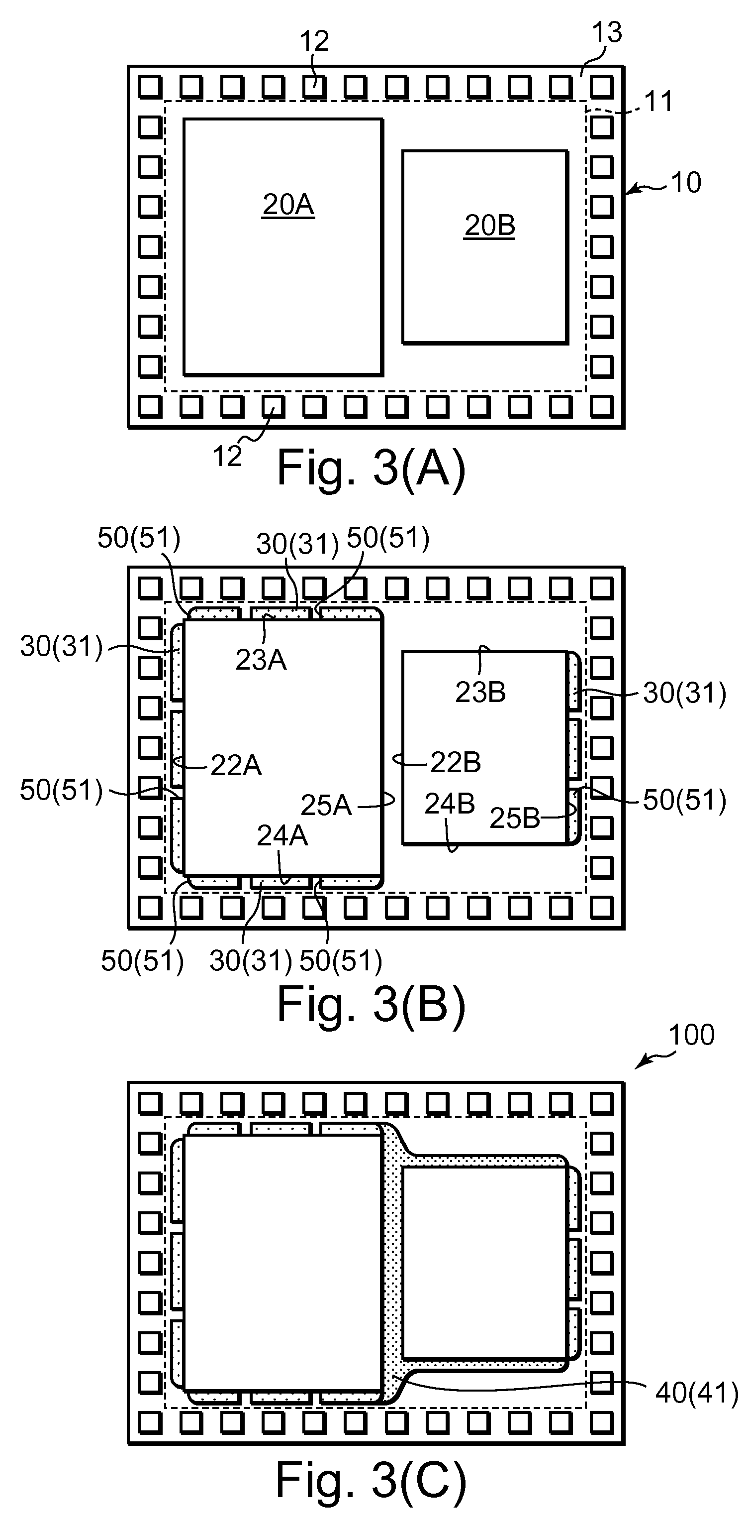
[0025]FIG. 1 is a schematic plan view showing a semiconductor device according to a first embodiment of the present invention. FIG. 2 is a schematic cross-sectional view illustrating the semiconductor device according to the first embodiment. FIG. 2 is a cross-sectional view taken along line A-A of FIG. 1.

[0026]As shown in FIGS. 1 and 2, the semiconductor device 100 according to the present embodiment includes an interposer 10 (mounting board) having a chip mounting area 11, an outer peripheral area 13 that surrounds the chip mounting area 11, and pads 12 formed in the outer peripheral area 13 as external terminals at predetermined intervals, all of which are provided within a main surface. Wirings or the like respectively connected to the pads 12 used as the external terminals, which are formed over the chip mounting area 13 and the outer peripheral area 13, are also provided in the interposer 10.

[0027]For instance, a first semiconductor chip 20A (semiconductor chip) provided with ...

second preferred embodiment

[0059]Incidentally, FIG. 5 is a schematic plan view showing a semiconductor device according to a second embodiment. FIG. 6 is a schematic cross-sectional view showing the semiconductor device according to the second embodiment. FIG. 6 is a cross-sectional view taken along line B-B of FIG. 5.

[0060]The present embodiment has explained the form in which the two semiconductor chips 20A and 20B are both provided with the first underfill 30 (or liquid first underfill 31). However, in the case of such a form in which a plurality of semiconductor chips are mounted, for example, semiconductor chips selected out of the plurality of semiconductor chips, at which the distances between all edge sides thereof and pads 12 of an interposer 10 increase sufficiently, need not to be provided with the first underfill 30.

[0061]Although the present embodiment has explained the form in which the charging and curing of the liquid first underfill 31 have been carried out simultaneously, such a form that th...


PUM


Abstract

The present invention provides a method for manufacturing a semiconductor device, which is capable of suppressing an overflow of a sealing resin and obtaining good sealing quality, simply and at low cost. Further, the present invention provides a semiconductor device that suppresses an overflow of a sealing resin and has good sealing quality, simply and at low cost. Liquid first underfill higher in viscosity than liquid second underfill is charged into space defined between a corresponding edge side of four edge sides of each of semiconductor chips, at which the distance between at least one edge side and each of pads opposite thereto, of an interposer is of the shortest, and the interposer. The liquid first underfill is cured and sealed with first underfill. Thereafter, the liquid second underfill is charged into space defined between the semiconductor chip and the interposer excluding the space sealed with the first underfill. The liquid second underfill is cured and sealed with second underfill.

Description

BACKGROUND OF THE INVENTION[0001]The present invention relates to a semiconductor device packaged by mounting semiconductor chips over a mounting board, and a method for manufacturing the semiconductor device.[0002]With greater functioning and miniaturization of small-sized electronic equipment typified by a cellular phone or the like, there has recently been an increasingly demand for a semiconductor device, a so-called SiP (System in Package) packaged by mounting a plurality of semiconductor chips and chip parts such as passive elements over a mounting board called an interposer in high density.[0003]However, there is a need to make the mounting board as small in size as possible for the purpose of high-density packaging. A reduction in the difference between the outer shape of the mounted semiconductor chip and the outer shape of the mounting board is required.[0004]The space between the mounting board and the semiconductor chip is normally sealed with a sealing resin called unde...

Claims


Application Information

Patent Timeline
Patent Type & Authority Applications(United States)
IPC IPC(8): H01L21/00
CPCH01L21/563H01L25/0655H01L2224/92125H01L2224/27013H01L2224/73204H01L2224/32225H01L2224/16225H01L2924/01078H01L2224/73203H01L2924/00012H01L2924/00H01L2224/83007H01L2224/83051H01L2224/83104H01L2224/83141H01L2924/00011H01L2924/00014H01L2224/0401H01L21/56
Inventor SHIZUNO, YOSHINORI
Owner LAPIS SEMICON CO LTD
Why Eureka
Try Eureka