Light emitting device

a technology of light emitting devices and shields, which is applied in the direction of solid-state devices, lasers, semiconductor light emitting elements, etc., can solve the problems of reducing the distance between the mounting location of the semiconductor light emitting element or the protective element and the pad portion, reducing the strength of the metal plate, and reducing the strength of the package, so as to prevent the effect of defects and improving the reliability of the light emitting devi

Active Publication Date: 2008-04-10
NICHIA CORP
View PDF1 Cites 36 Cited by
  • Summary
  • Abstract
  • Description
  • Claims
  • Application Information

AI Technical Summary

Benefits of technology

[0016]Accordingly, a package resin can be prevented from flowing into the groove portion. Therefore, the defect can be prevented from occurring in the process.
[0017]According to the present invention, in a light emitting device comprising a semiconductor light emitting element and an optional protect...

Problems solved by technology

However, when such a pad portion is provided at an end portion of a lead electrode constituting the terminal electrode, a distance between the mounting location of the semiconductor light emitting element or the protective element and the pad portion becomes too large.
However, in such cases, not only the strength of the metal plate, but also the strength of the package decreases.
Further, the heat dissipation also decreases so that high output power cannot be achie...

Method used


Image

  • Light emitting device
  • Light emitting device
  • Light emitting device

Examples


Embodiment Construction

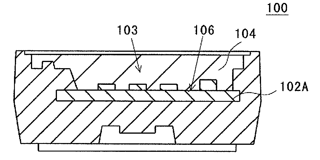
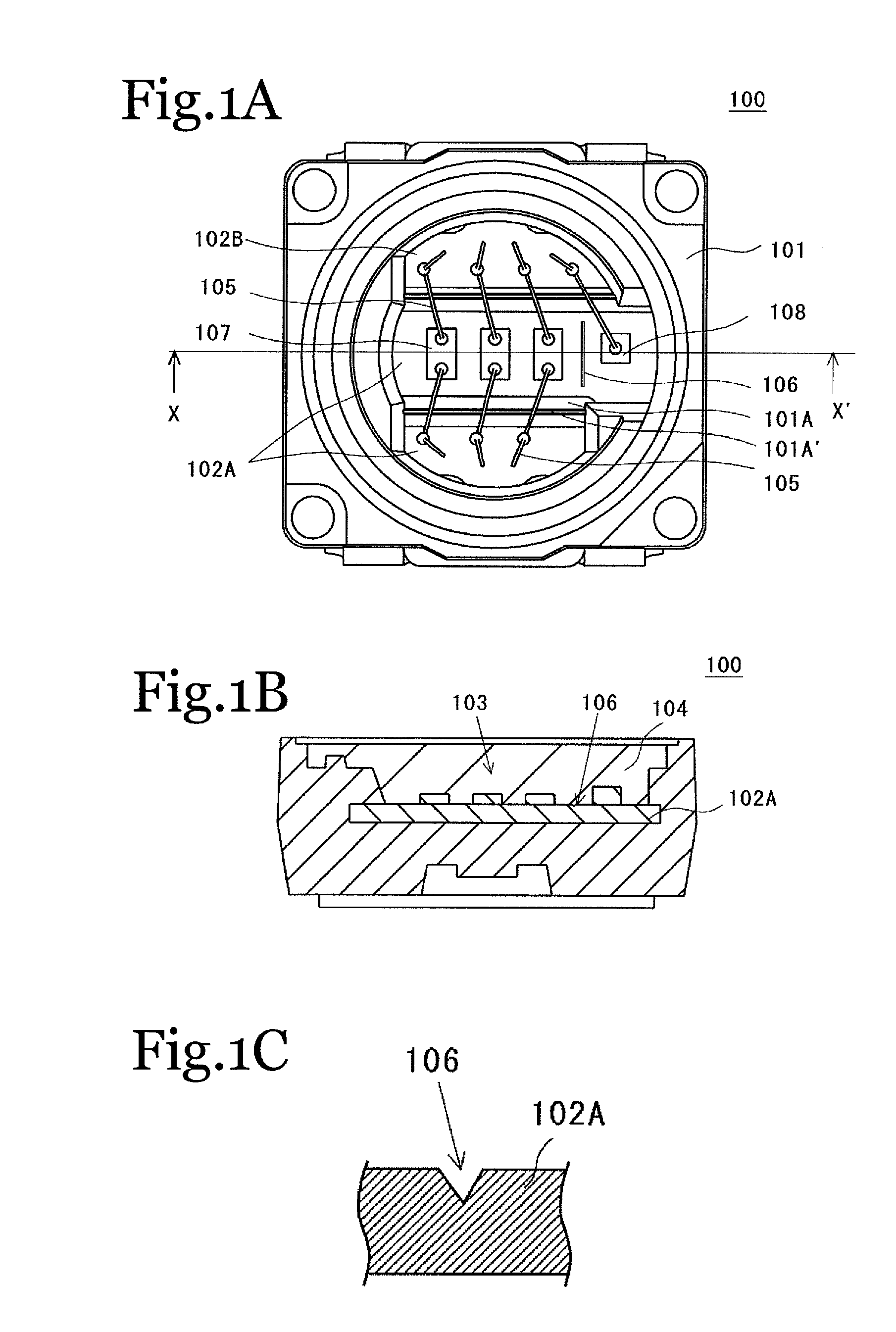
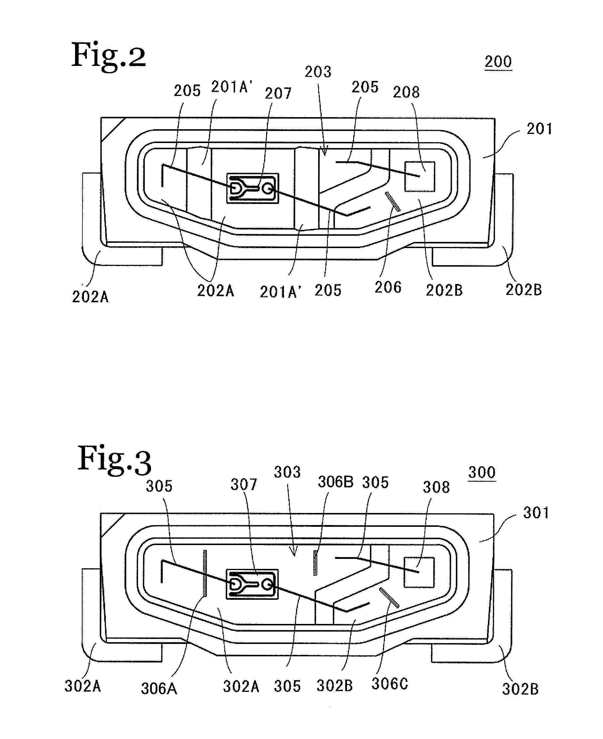
[0028]The preferred embodiments of the present invention will be described below with reference to the accompanying drawings.

[0029]Herein, the form of the following embodiments are intended as examples of a light emitting device that are representative of the technology behind the present invention, and any limitation of the scope of the invention by the embodiments is not intended. In addition, the present specification will by no means limit the members described in claims to the members described in the embodiments. Especially, size, material, shape, and the relative configuration etc. of the components described in the preferred embodiments are for illustration purpose only, and do not intend to limit the invention therein, unless specifically described. In the drawings, the size and the positional relationship of the components may be exaggerated for clarity.

[0030]Further, in the description below, identical members or members of the same quality are assigned the same names and...


PUM


Abstract

A light emitting device includes a package having a recess defined by an inner wall and a bottom surface and a lead terminal exposed at the bottom surface of the recess and protruded outward from the package. The lead terminal exposed at the bottom surface of the recess portion including a semiconductor light emitting element mounting region and a wire connecting region for connecting a conductive wire from the semiconductor light emitting element thereto. At least one of regions between the semiconductor light emitting element mounting region and the wire connecting region has a groove portion disposed in a position spaced apart from a peripheral edge portion of the lead terminal that is exposed at the bottom surface of the recess.

Description

BACKGROUND OF THE INVENTION[0001]1. Field of the Invention[0002]The present invention relates to a light emitting device that can be used in an indicator, a lighting apparatus, a display, a backlight for liquid crystal display etc. More particularly, the present invention relates to a light emitting device that is highly reliable by employing a protective device even when a semiconductor light emitting element having high output is mounted thereon.[0003]2. Background Information[0004]For example, a chip type light-emitting element disclosed in Japanese Laid-Open Patent Application No. 11-54804 comprises an insulating substrate, a pair of terminal electrodes provided on both end parts of the surface of the substrate, a semiconductor light emitting element mounted on one of the terminal electrodes, and a protective element for protecting the semiconductor light emitting element from at least the reverse voltage that may be applied thereto. The protective element is mounted on the othe...

Claims


Application Information

Patent Timeline
IPC IPC(8): H01L33/00H01L33/28H01L33/32H01L33/48H01L33/56H01L33/62
CPCH01L24/48H01L25/0753H01L2924/19107H01L2224/4911H01L2924/10329H01L25/167H01L33/483H01L33/62H01L2224/48097H01L2224/48247H01L2924/01012H01L2924/01013H01L2924/0102H01L2924/01025H01L2924/01029H01L2924/0103H01L2924/01032H01L2924/01038H01L2924/01046H01L2924/01047H01L2924/0105H01L2924/01056H01L2924/01057H01L2924/01058H01L2924/01059H01L2924/0106H01L2924/01063H01L2924/01078H01L2924/01079H01L2924/01082H01L2924/014H01S5/005H01S5/02208H01S5/02276H01L2924/01005H01L2924/01006H01L2924/01019H01L2924/01021H01L2924/01023H01L2924/01024H01L2924/01033H01L2924/0104H01L2924/01065H01L2924/01066H01L2924/01067H01L2924/01068H01L2924/01074H01L2924/01322H01L2924/00H01L2224/45144H01L2224/45124H01L2224/45147H01L2224/45169H01L2924/00014H01L2924/12035H01L24/45H01L2924/181H01L24/49H01S5/02345H01S5/0087H01S5/02234H01S5/4025H01L2224/05599
Inventor BANDO, YOSHITAKANAKASHIMA, SHINTAROTAKAO, TOSHIMASA
Owner NICHIA CORP
Why Eureka
Try Eureka