Jitter generating device and phase modulating device

a jitter generation and phase modulating technology, applied in the direction of demodulation, angle modulation, electric devices, etc., can solve the problems of increasing technical burden, requiring cost and space, and difficult to faithfully implement i(t) and q(t) signals, so as to achieve low cost and low cost. , the effect of low cos

Inactive Publication Date: 2008-04-17
YOKOGAWA ELECTRIC CORP
View PDF1 Cites 2 Cited by
  • Summary
  • Abstract
  • Description
  • Claims
  • Application Information

AI Technical Summary

Benefits of technology

[0039]According to the phase modulation generating device, the carrier signal generated by the carrier signal generator is phase-modulated by the orthogonal modulator, and furthermore, the voltage value of the DC voltage is corrected synchronously with the modulation signal, so that the amplitude of the signal output from the orthogonal modulator comes to be constant. Therefore, it is possible to obtain a phase-modulated signal having a small modulation distortion at a low cost.
[0040]According to the jitter generating device in accordance with the invention, the carrier signal generated by the carrier signal generator is phase-modulated by the orthogonal modulator, and furthermore, the amplitude of the output signal is caused to be constant by the limiter amplifier. Therefore, it is possible to obtain a phase-modulated signal having a small modulation distortion at a low cost.
[0041]According to the phase modulating device in accordance with the present invention, the carrier signal generated by the carrier signal generator is phase-modulated by the orthogonal modulator, and furthermore, the voltage value of the DC voltage is corrected synchronously with the modulation signal, so that the amplitude of the signal output from the orthogonal modulator comes to be constant. Therefore, it is possible to obtain a phase-modulated signal having a small modulation distortion at a low cost.

Problems solved by technology

Both of them are to generate a carrier signal frequency or a signal having a high frequency which is close to the carrier signal frequency, and a cost and a space are required.
Therefore, a technical burden is increased.
Consequently, both I(t) and Q(t) include an infinite harmonic content of a frequency p and it is hard to faithfully implement the I(t) and Q(t) signals.

Method used


Image

  • Jitter generating device and phase modulating device
  • Jitter generating device and phase modulating device
  • Jitter generating device and phase modulating device

Examples


Embodiment Construction

[0049]An exemplary embodiment of a phase modulating device according to the invention will be described below with reference to FIGS. 1 to 6.

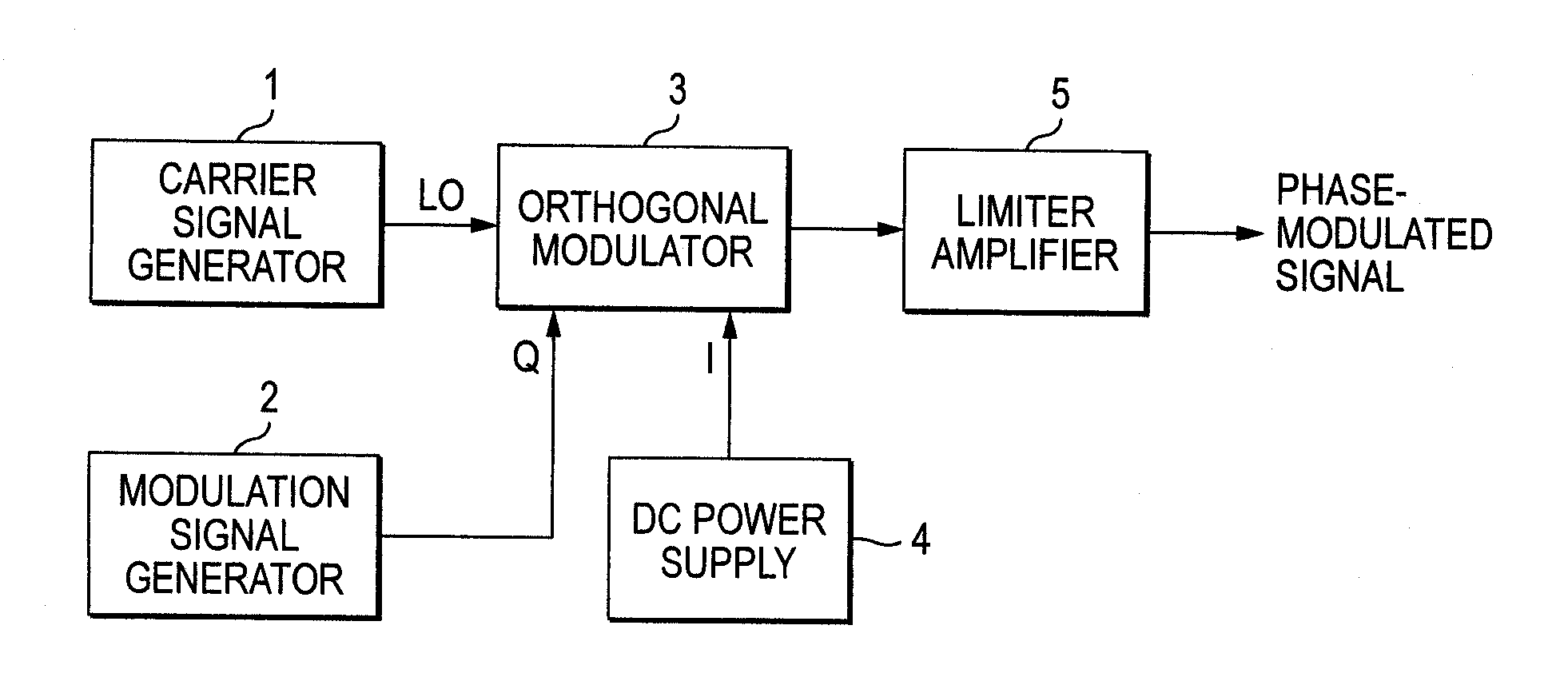
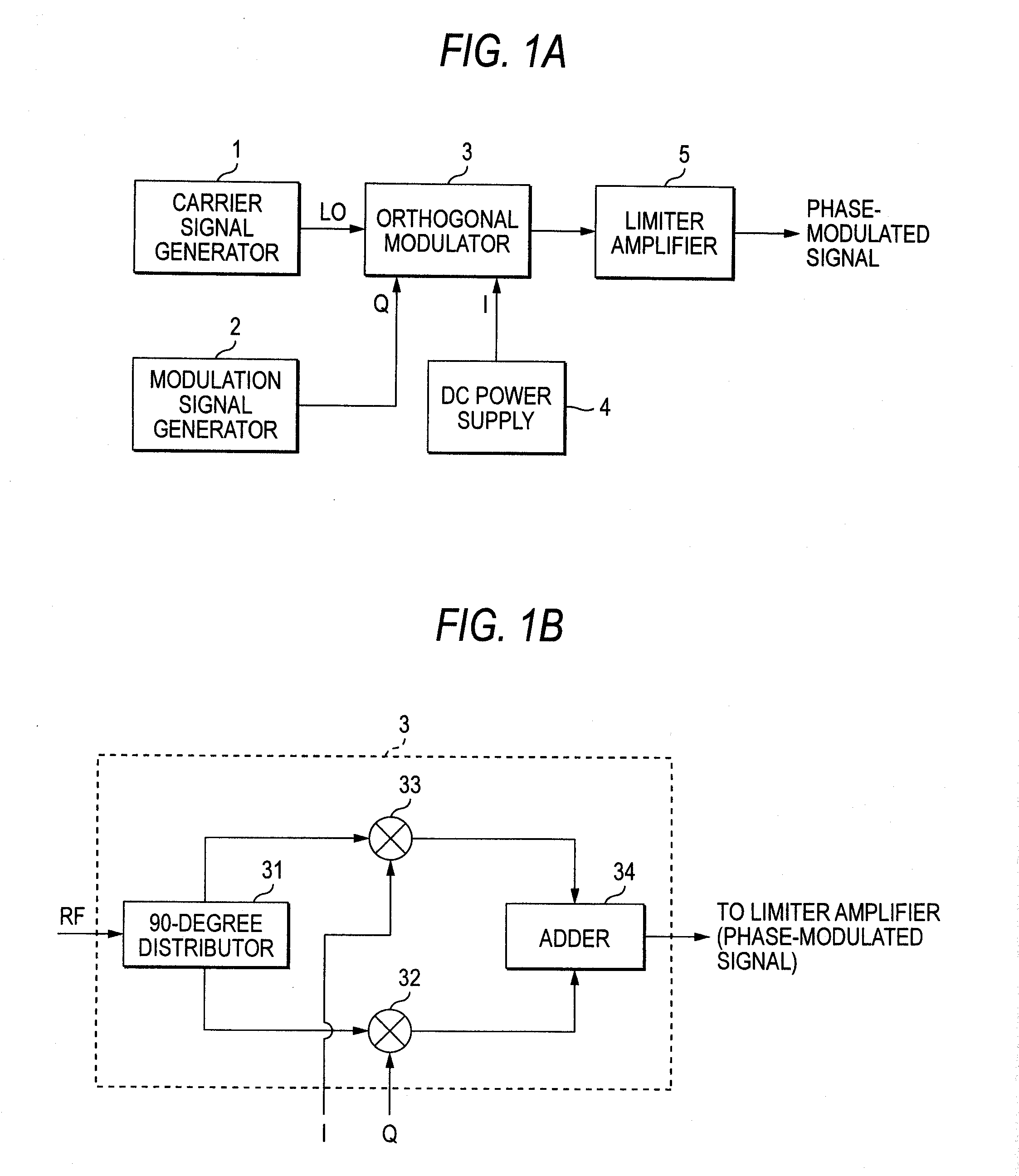
[0050]FIG. 1A is a block diagram showing a structure according to an exemplary embodiment of the phase modulating device in accordance with the present invention.

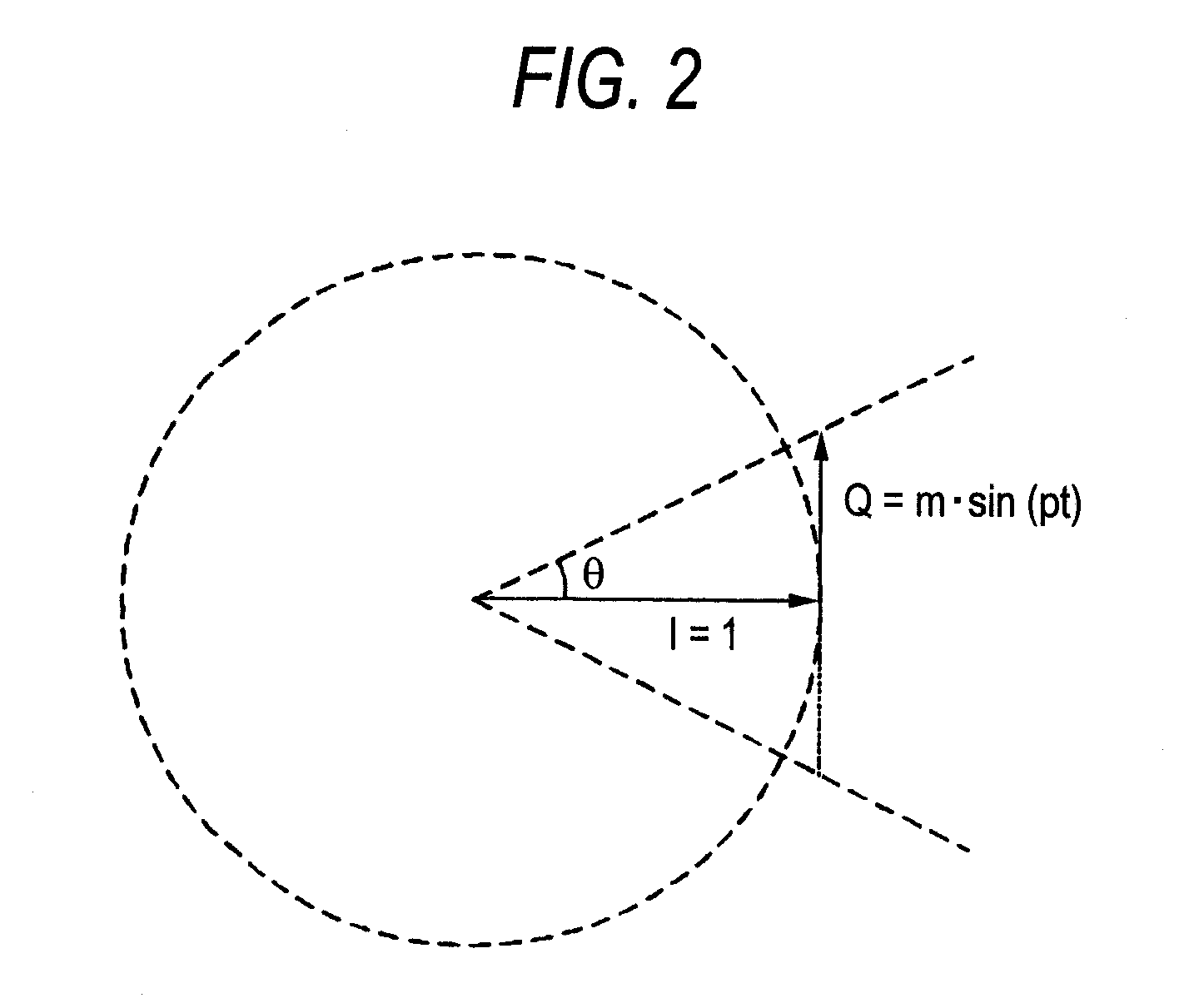
[0051]As shown in FIG. 1A, a phase modulating device according to the exemplary embodiment includes: a carrier signal generator 1 for outputting a carrier signal having a frequency ω; a modulating signal generator 2 for outputting a modulation signal P=m·sin(pt); an orthogonal modulator 3; a DC power supply 4 for applying a DC voltage to the orthogonal modulator 3; and a limiter amplifier 5 (amplitude adjustment means) for amplifying a signal output from the orthogonal modulator 3 and adjusting an amplitude thereof to be constant.

[0052]As shown in FIG. 1A, the carrier signal transmitted from the carrier signal generator 1 is input to an LO input terminal of the orthogonal modulator 3. ...


PUM


Abstract

A jitter generating device for generating a jitter on a carrier signal includes: a carrier signal generator for generating the carrier signal; a modulation signal generator for generating a modulation signal corresponding to the jitter; an orthogonal modulator for modulating a phase of the carrier signal generated by the carrier signal generator using the modulation signal generated by the modulation signal generator as one of modulation input signals; a DC power supply for applying a DC voltage serving as the other modulation input signal to the orthogonal modulator; and a limiter amplifier for setting an amplitude of an output signal of the orthogonal modulator to be constant.

Description

[0001]This application is based on and claims priority from Japanese Patent Application No. 2006-277434, filed on Oct. 11, 2006, the entire contents of which are hereby incorporated by reference.BACKGROUND OF THE INVENTION[0002]1. Technical Field[0003]The present disclosure relates to a jitter generating device for generating a jitter on a carrier signal and a phase modulating device for modulating a phase of the carrier signal, and more particularly to a jitter generating device and a phase modulating device which have a broad band.[0004]2. Related Art[0005]For example, in a performance inspection of a communication device, a broadband jitter generating device has been required. For a related-art jitter generating device, as shown in FIG. 7A, there has been known a device that adds in an adder 23, a signal of a carrier signal generator 21 and that of a signal generator 22 having, as an oscillation frequency, a sum (ω+p) of a carrier signal frequency (ω) and a modulation signal freq...

Claims


Application Information

Patent Timeline
Patent Type & Authority Applications(United States)
IPC IPC(8): H03C3/00
CPCH03D7/00
Inventor MAEDA, MINORU
Owner YOKOGAWA ELECTRIC CORP
Why Eureka
Try Eureka