Thin film transistor array substrate and repair method thereof

a thin film transistor array and liquid crystal display technology, applied in non-linear optics, instruments, optics, etc., can solve the problem that the repair of the pixel is not easy to be found, and achieve the effect of enhancing the yield of the product and reducing the repair tim

Inactive Publication Date: 2008-04-17
CHUNGHWA PICTURE TUBES LTD
View PDF8 Cites 41 Cited by
  • Summary
  • Abstract
  • Description
  • Claims
  • Application Information

AI Technical Summary

Benefits of technology

[0011]One object of the present invention provides a thin film transistor array substrate and repair method thereof for liquid crystal display device. This pixel structure of the thin film transistor array substrate only needs to irradiate one laser beam to complete the repair. The brightness of the repaired pixel is not displaying the gray defect but as same as the previous regular pixel, wherein the repaired pixel is not easy to be found out. The pixel structure can substantially reduce the repair time and enhance the yield of the product.

Problems solved by technology

The brightness of the repaired pixel is not displaying the gray defect but as same as the previous regular pixel, wherein the repaired pixel is not easy to be found out.

Method used


Image

  • Thin film transistor array substrate and repair method thereof
  • Thin film transistor array substrate and repair method thereof
  • Thin film transistor array substrate and repair method thereof

Examples


Embodiment Construction

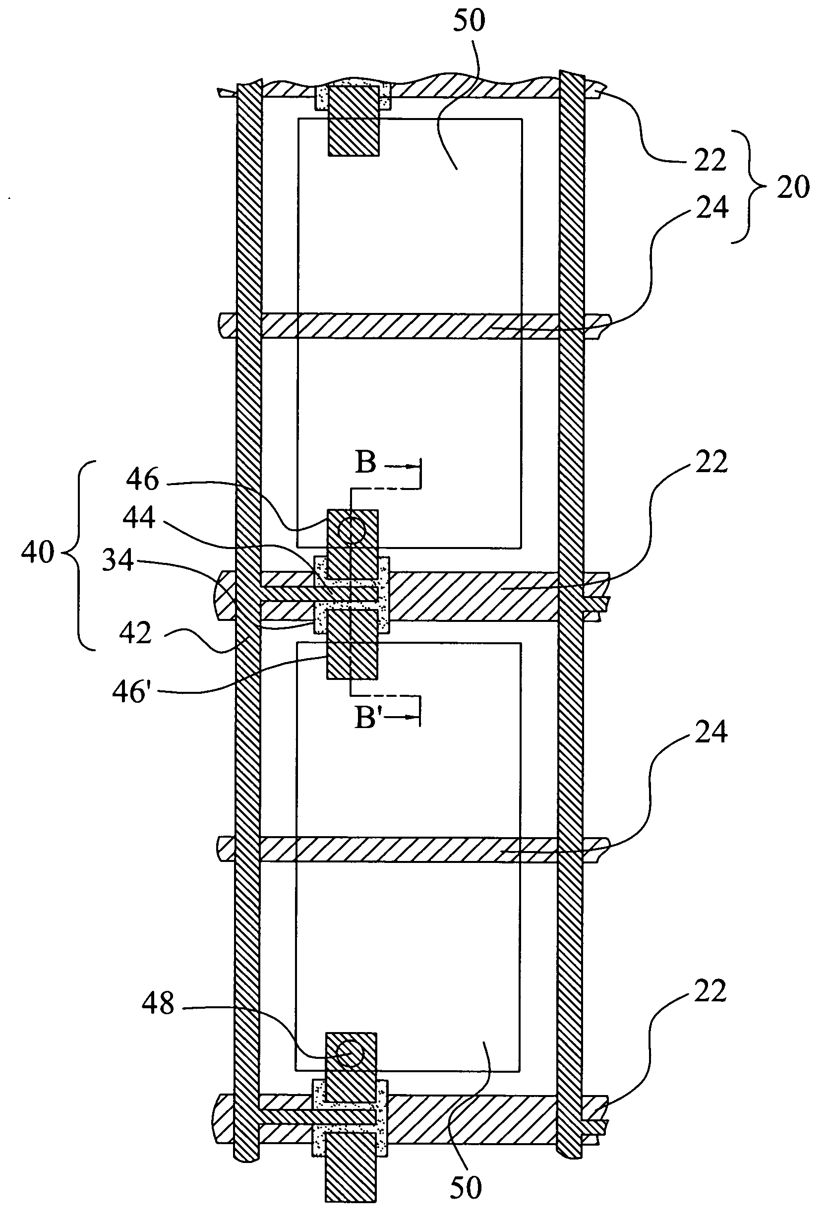
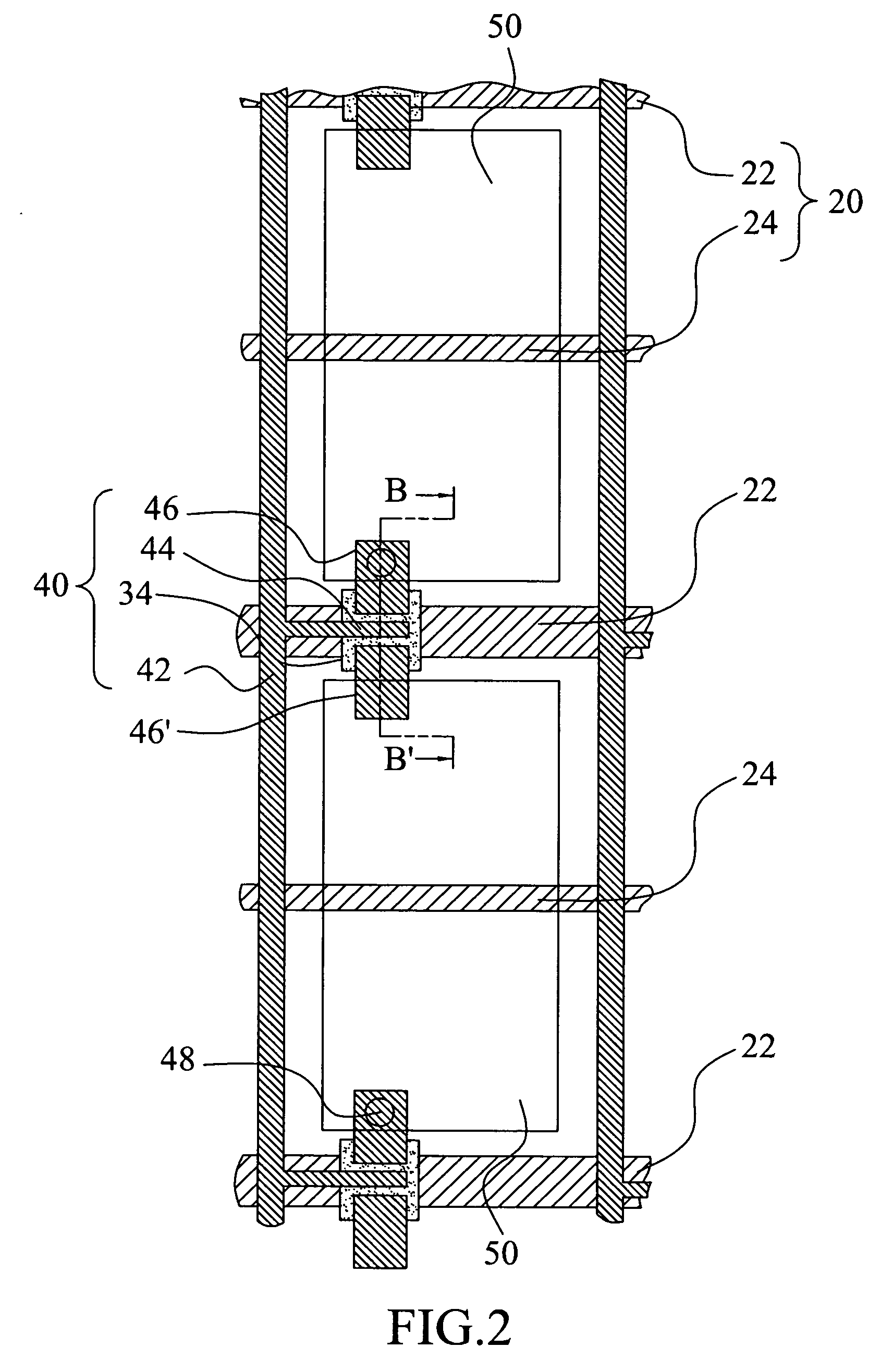
[0020]FIG. 2 is a plan view of the pixel structure illustrating one embodiment of the present invention. Such as shown in FIG. 2, in the present embodiment, a plurality of scan lines 22 and a plurality of data lines 42 are disposed on a substrate (not shown in FIG. 2). Scan lines 22 and data lines 42 cross each other to define a plurality of pixel areas. There are a plurality of storage capacitance lines 24 are disposed extend over pixel areas along scan lines 22 and to cross data lines 42. A plurality of pixel electrodes 50 are respectively disposed on each of pixel areas and a plurality of thin film transistors 40 are respectively disposed on the each scan lines 22 inside the each pixel areas. Wherein, any one of thin film transistors includes a gate electrode (not shown in FIG. 2); a source electrode 44; a first drain electrode 46; and a second drain electrode 46′. The gate electrode is as a portion of the each scan lines 22, the source electrode 44 is over the gate electrode and...


PUM

PropertyMeasurementUnit
electricallyaaaaaaaaaa
insulatingaaaaaaaaaa
storage capacitanceaaaaaaaaaa

Abstract

A thin film transistor array substrate includes a plurality of pixel areas defined by scan lines and data lines; a pixel electrode disposed on each of pixel areas; and a thin film transistor disposed on the each scan lines includes a gate electrode; a source electrode; a first drain electrode and a second drain electrode disposed along the source electrode and on the opposite sides; and an insulating layer over the source electrode, the first drain electrode, the second drain electrode and data lines. The insulating layer has a contact hole to electrically connect with the pixel electrode and the first drain electrode; and the second drain electrode extends to a portion adjacent the pixel electrode and electrically insulated with each other by the insulating layer. The present repair method is to irradiate a laser beam to short the second drain electrode and the pixel electrode at the adjacent pixel area.

Description

BACKGROUND OF THE INVENTION[0001]1. Field of the Invention[0002]The present invention generally relates to a liquid crystal display device, and more particularly relates to a thin film transistor array substrate and repair method thereof for a liquid crystal display device.[0003]2. Description of the Prior Art[0004]Currently, the thin film transistor liquid crystal display (TFT LCD) is the most popular plane display device. It has many advantages such as its low consumption, thin and compact shape, and low driving voltage, etc. Generally, a TFT LCD panel has a liquid crystal layer sandwiched by two substrates with electrodes thereof. Applying voltages to respect electrodes can control the light transmittance of the liquid crystal. The display region of a TFT panel is composed of a plurality of matrix-like pixels.[0005]During the procedures of fabricating the TFT panel, the pixel is liable to be damaged and resulted in an abnormal short-circuit or open-circuit by several factors such...

Claims


Application Information

Patent Timeline
Patent Type & Authority Applications(United States)
IPC IPC(8): G02F1/136
CPCG02F1/136227G02F2001/136268G02F1/136259G02F1/136268
Inventor LIN, KUANG-HSIANGYU, HUEI-CHUNG
Owner CHUNGHWA PICTURE TUBES LTD
Why Eureka
Try Eureka