Gas distribution assembly for use in a semiconductor work piece processing reactor

a technology for gas distribution and workpieces, which is applied in the direction of coatings, metallic material coating processes, chemical vapor deposition coatings, etc., can solve the problems of gap filling performance and reducing ozone concentration

Active Publication Date: 2008-04-24
ADVANCED MICRO FAB EQUIP INC CHINA
View PDF13 Cites 380 Cited by
  • Summary
  • Abstract
  • Description
  • Claims
  • Application Information

AI Technical Summary

Benefits of technology

[0002]The present invention relates to a gas distribution assembly for use in a semiconductor work piece processing reactor, and more specifically to a gas distribution assembly which, when installed within a semiconductor work piece processing reactor, is operable to deliver gaseous chemicals to a semiconductor work piece for purposes of depositing uniform films or layers on the surface of the semiconductor work piece by chemical vapor deposition, atomic layer deposition or the like.
[0002]The present invention relates to a gas distribution assembly for use in a semiconductor work piece processing reactor, and more specifically to a gas distribution assembly which, when installed within a semiconductor work piece processing reactor, is operable to deliver gaseous chemicals to a semiconductor work piece for purposes of depositing uniform films or layers on the surface of the semiconductor work piece by chemical vapor deposition, atomic layer deposition or the like.

Problems solved by technology

However, higher temperatures experienced within the showerhead typically reduces the Ozone concentration since the half-life time of this chemical is strongly temperature dependent.
This production of particles within the showerhead can potentially deteriorate the resulting gap fill performance of the resulting oxide film in an integrated circuit construction, if these polymeric particles are deposited on the semiconductor work piece surface.

Method used


Image

  • Gas distribution assembly for use in a semiconductor work piece processing reactor
  • Gas distribution assembly for use in a semiconductor work piece processing reactor
  • Gas distribution assembly for use in a semiconductor work piece processing reactor

Examples


Embodiment Construction

[0025]This disclosure of the invention is submitted in furtherance of the constitutional purposes of the U.S. Patent Laws “to promote the progress of science and useful arts” (Article 1, Section 8).

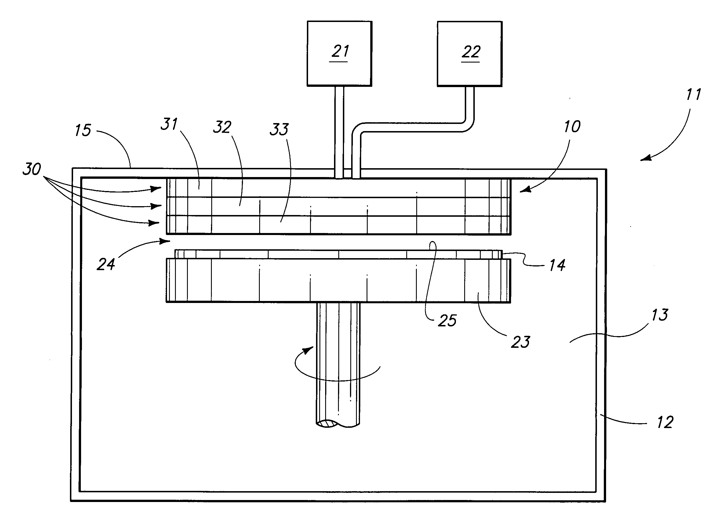
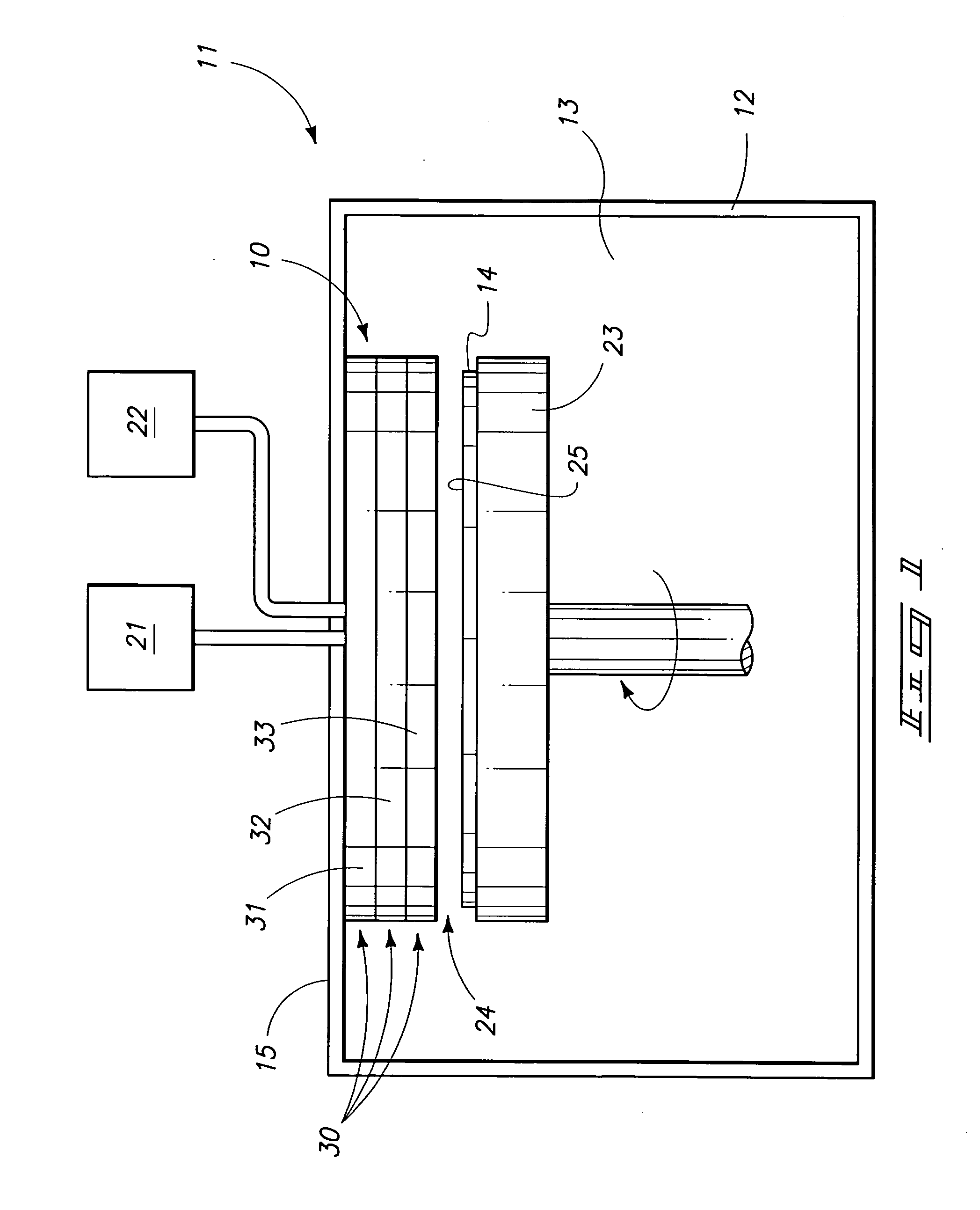
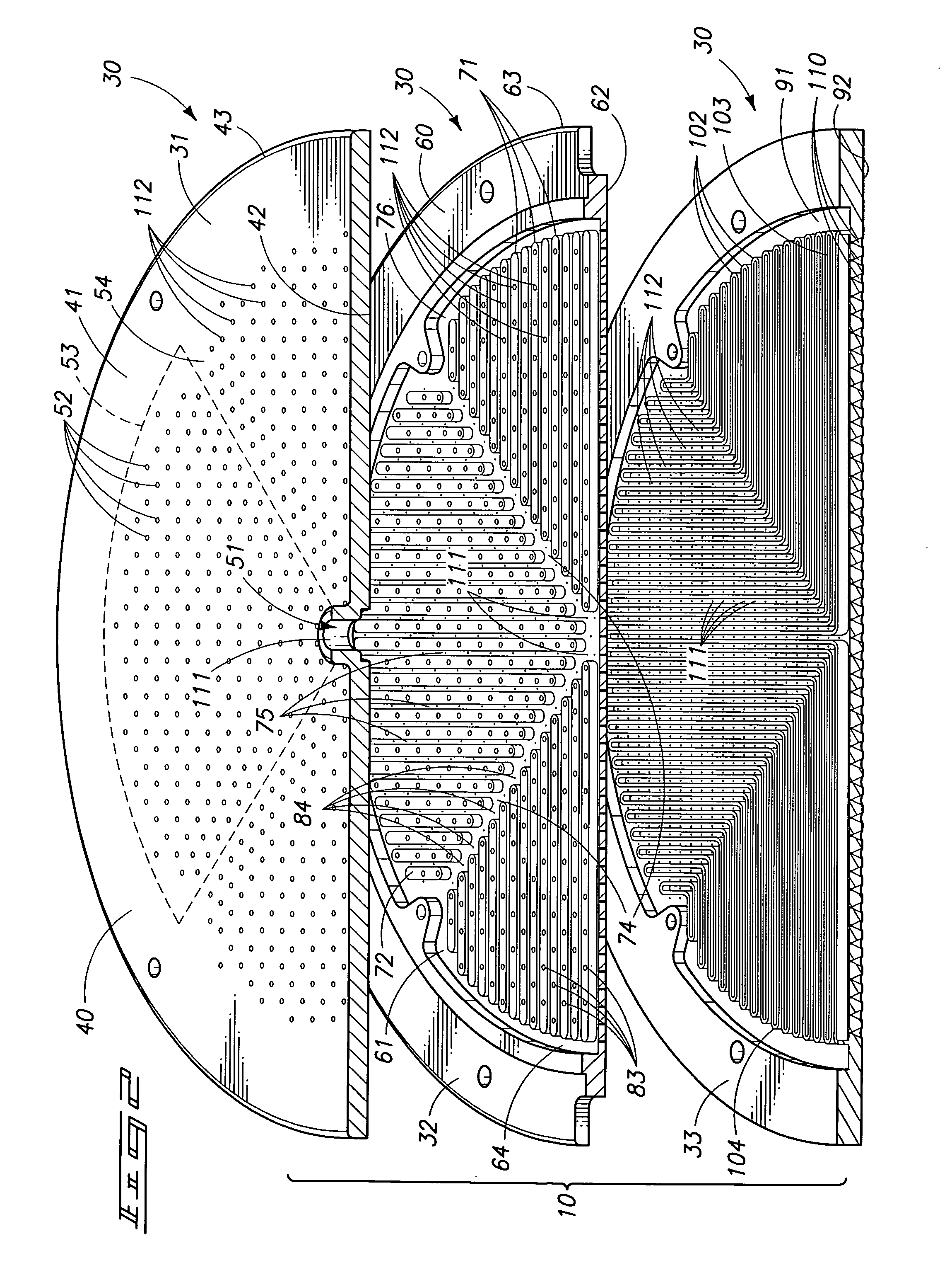
[0026]A gas distribution assembly 10 for use in a semiconductor work piece processing reactor is seen in the greatly simplified view of FIG. 1. The present invention may be used for both chemical and vapor deposition (CVD); or atomic layer deposition (ALD) as will become more apparent in the paragraphs which follow. As illustrated therein, the gas distribution assembly 10 is incorporated or otherwise positioned within a processing chemical vapor deposition (CVD) chamber and which is generally designated by the numeral 11. The processing or CVD chamber 11 has a circumscribing sidewall 12 which defines an internal chamber 13, and which receives and processes a semiconductor wafer, or semiconductor work piece which is generally designated by the numeral 14. In the arrangement as seen in FIG....


PUM

PropertyMeasurementUnit
surface areaaaaaaaaaaa
semiconductoraaaaaaaaaa
thermalaaaaaaaaaa

Abstract

A semiconductor work piece processing reactor is described and which includes a processing chamber defining a deposition region; a pedestal which supports and moves a semiconductor work piece to be processed within the deposition region of the processing chamber; and a gas distribution assembly mounted within the processing chamber and which defines first and second reactive gas passageways which are separated from each other, and which deliver two reactant gases to a semiconductor work piece which is positioned near the gas distribution assembly.

Description

RELATED PATENT DATA[0001]This application claims priority from Chinese Patent Application Serial No. 200610117260.2, and which was filed on Oct. 18, 2006.TECHNICAL FIELD[0002]The present invention relates to a gas distribution assembly for use in a semiconductor work piece processing reactor, and more specifically to a gas distribution assembly which, when installed within a semiconductor work piece processing reactor, is operable to deliver gaseous chemicals to a semiconductor work piece for purposes of depositing uniform films or layers on the surface of the semiconductor work piece by chemical vapor deposition, atomic layer deposition or the like.BACKGROUND OF THE INVENTION[0003]Chemical vapor deposition and atomic layer deposition are critical manufacturing steps in semiconductor fabrication. In particular, the deposition of oxide films is an important component in the fabrication of integrated circuits. More specifically, it has long been known that thermal processing must typi...

Claims


Application Information

Patent Timeline
Patent Type & Authority Applications(United States)
IPC IPC(8): C23F1/00C23C16/00
CPCC23C16/45574C23C16/45565
Inventor CHEN, AIHUAWANG, SHULINHO, HENRYYIN, GERALDLV, QINGFU, LI
Owner ADVANCED MICRO FAB EQUIP INC CHINA
Why Eureka
Try Eureka