Semiconductor device and method of manufacturing semiconductor device

Inactive Publication Date: 2008-04-24
RENESAS ELECTRONICS CORP
View PDF5 Cites 3 Cited by
  • Summary
  • Abstract
  • Description
  • Claims
  • Application Information

AI Technical Summary

Benefits of technology

[0024]According to the present invention, a highly-reliable semiconductor device is successfully prevented from causing cracks and from being de

Problems solved by technology

The conventional semiconductor device 7 has been suffering from a risk of caus

Method used


Image

  • Semiconductor device and method of manufacturing semiconductor device
  • Semiconductor device and method of manufacturing semiconductor device
  • Semiconductor device and method of manufacturing semiconductor device

Examples


Embodiment Construction

[0032]The invention will now be described herein with reference to illustrative embodiments. Those skilled in the art will recognize that many alternative embodiments can be accomplished using the teachings of the present invention and that the invention is not limited to the embodiment illustrated for explanatory purposes.

[0033]Paragraphs below will describe embodiments of the present invention referring to the attached drawings. It is to be understood that any common constituents will be given with similar reference numerals in all drawings, and explanations therefore will not be repeated.

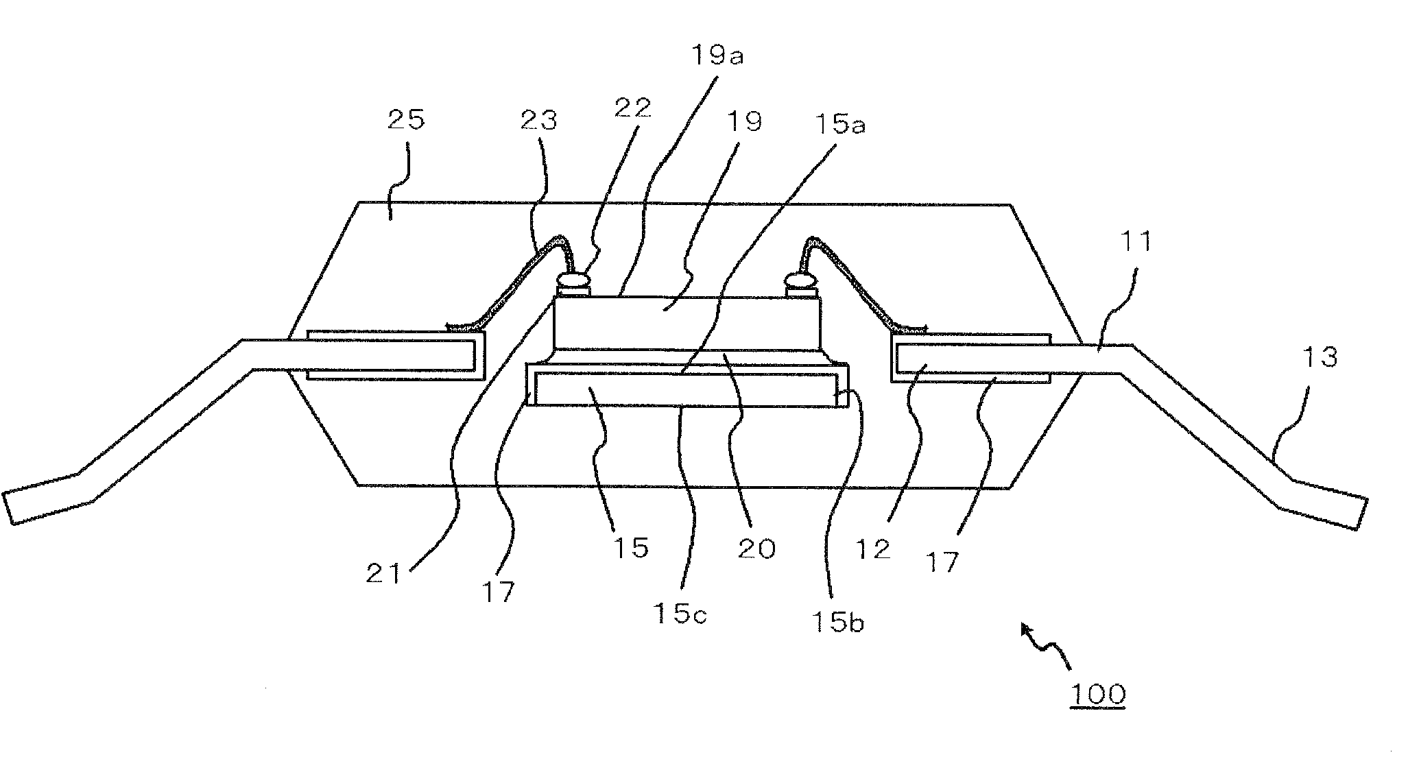
[0034]FIG. 1 is a sectional view schematically showing a semiconductor device according to an embodiment of the present invention. A semiconductor device 100 of this embodiment has a lead frame 11 which has an island portion 15 having a roughened upper surface 15a and side faces 15b, and an unroughened lower surface 15c, and a plurality of leads having roughened inner lead portions (inner leads 1...


PUM


Abstract

A semiconductor device of the present invention includes a lead frame having an island portion having a roughened upper surface and side faces, and an unroughened lower surface, and also having a plurality of leads having roughened inner lead portions and unroughened outer lead portions; a semiconductor chip placed on the upper surface of the island portion of the lead frame; a plurality of electrode pads provided on the upper surface of the semiconductor chip; a plurality of wires connecting the plurality of electrode pads and the plurality of leads; and a resin molding the semiconductor chip.

Description

[0001]This application is based on Japanese patent application No. 2006-283393 the content of which is incorporated hereinto by reference.BACKGROUND[0002]1. Technical Field[0003]The present invention relates to a semiconductor device and a method of manufacturing a semiconductor device, and in particular to a resin-molded semiconductor device using a lead frame, and a method of manufacturing the same.[0004]2. Related Art[0005]Before describing of the present invention, the related art will be explained in detail with reference to FIGS. 5 and 6 in order to facilitate the understanding of the present invention.[0006]A conventional semiconductor device 7 shown in FIG. 5 contains a lead frame 1, a semiconductor chip 4 placed on an island portion 2 of the lead frame 1 while placing an adhesive 3 in between, a plurality of wires 5 respectively connecting a plurality of electrodes of the semiconductor chip 4 and a plurality of leads of the lead frame 1, and a resin 6 molding the semiconduc...

Claims


Application Information

Patent Timeline
IPC IPC(8): H01L21/02H01L23/495
CPCH01L23/3107H01L2924/01006H01L23/49548H01L23/49582H01L24/32H01L24/45H01L2224/32245H01L2224/45144H01L2224/48091H01L2224/48247H01L2224/48465H01L2224/73265H01L2224/85444H01L2224/92H01L2224/92247H01L2924/01029H01L2924/01046H01L2924/01078H01L2924/01079H01L2924/01082H01L2924/01088H01L23/49503H01L2924/01005H01L24/48H01L2924/01033H01L2924/15747H01L2924/01028H01L2924/00014H01L2924/00H01L2924/3512H01L2224/48644H01L2924/181H01L2924/00012
Inventor OKADA, SHIROUSHIGEMATSU, RYOICHI
Owner RENESAS ELECTRONICS CORP
Why Eureka
Try Eureka