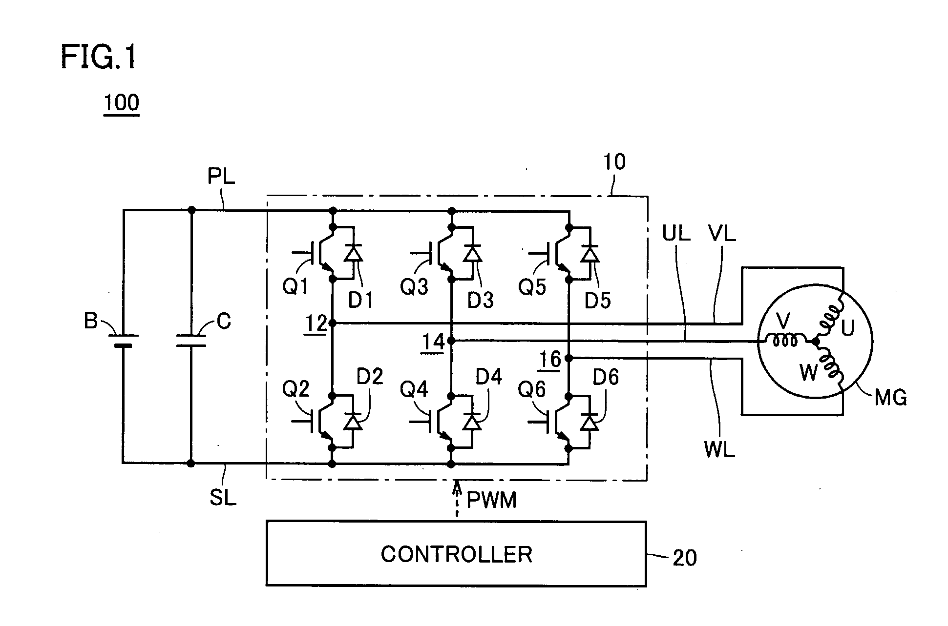
Semiconductor Module And Semiconductor Device
a technology of semiconductor devices and semiconductor modules, applied in semiconductor devices, semiconductor/solid-state device details, electrical apparatus, etc., can solve the problems of insufficient capacity of power devices at the center than the periphery, inability of power devices to have uniform temperature profiles, etc., to achieve uniform temperature profiles, reduce thickness, and reduce the effect of heat loss
- Summary
- Abstract
- Description
- Claims
- Application Information
AI Technical Summary
Benefits of technology
Problems solved by technology
Method used
Image

Examples
second embodiment
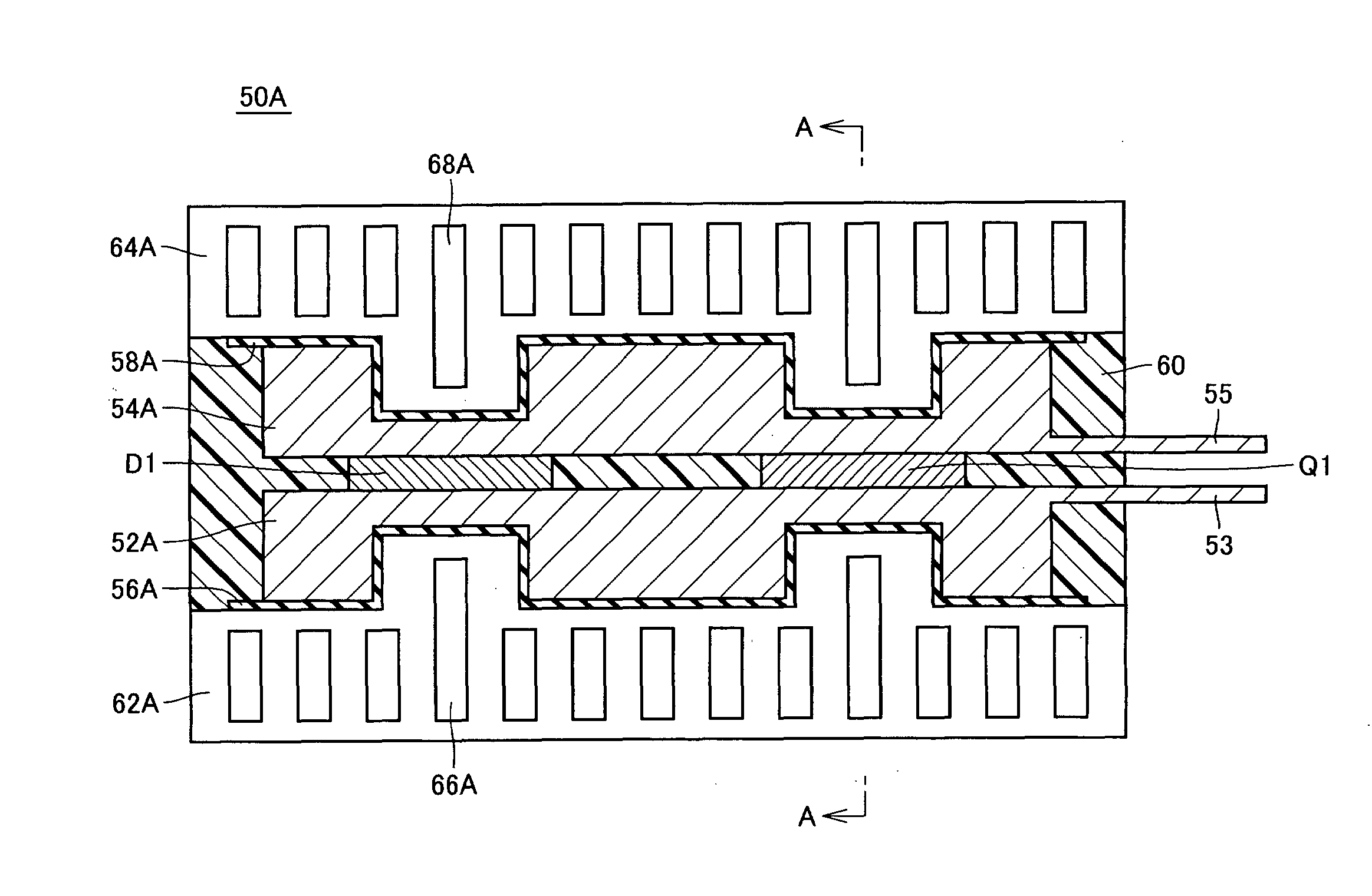
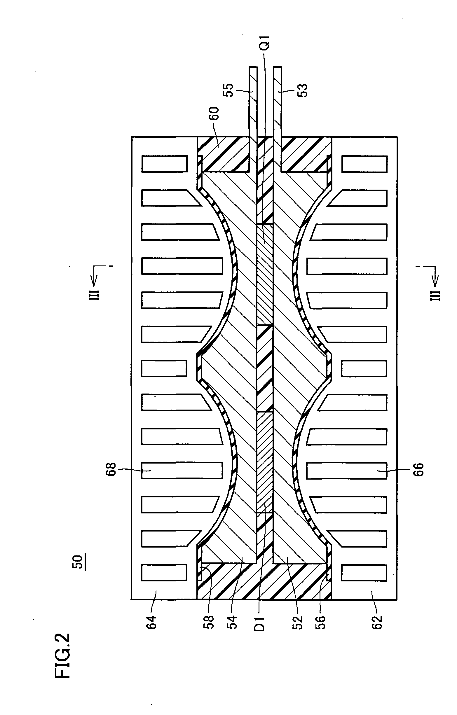
[0073]FIG. 5 is a cross section of a structure of a semiconductor module in a second embodiment of the present invention. Note that a load drive device including an inverter employing the semiconductor module of the second embodiment has the same circuit configuration as the FIG. 1 load drive circuit 100. Furthermore in the second embodiment each of upper and lower arms of each of U, V and W phase arms of the inverter is identically structured and accordingly FIG. 5 shows a structure of the U phase, upper arm of the inverter representatively. Furthermore FIG. 5 corresponds to FIG. 2 described in the first embodiment.
[0074] With reference to FIG. 5, a semiconductor module 50A corresponds in configuration to semiconductor module 50 described in the first embodiment with reference to FIG. 2 having electrode plates 52 and 54 and insulation plates 56 and 58 replaced with electrode plates 52A and 54A and insulation plates 56A and 58A.
[0075] Electrode plate 52A differs in geometry from e...
third embodiment
[0084]FIG. 8 is a cross section of a structure of a semiconductor device in a third embodiment of the present invention. With reference to the figure, a semiconductor device 51 includes power transistor Q1, diode D1, an electrode plate 52D, 54D, an insulation plate 56D, 58D, a resin mold 60, and a cooling element 62D, 64D.
[0085] Electrode plates 52D and 54D are disposed to sandwich power transistor Q1 and diode D1. In the third embodiment electrode plate 52D, 54D does not have such a geometry of electrode 52, 54 as described in the first embodiment with reference to FIG. 2. Rather, it is a typical, flat plate. Electrode plate 52D, 54D, as well as electrode plate 52, 54, is formed of a highly electrically and thermally conductive material, such as copper. Electrode plates 52D and 54D acts as electrodes as well as heat sinks transferring heat from power transistor Q1 and diode D1 to cooling elements 62D and 64D, respectively.
[0086] Insulation plate 56D is disposed between electrode ...
fourth embodiment
[0093]FIG. 9 is a cross section of a structure of a cooling element in a semiconductor device of a fourth embodiment of the present invention. The figure shows the cooling element in a cross section parallel to a plane opposite a power device for the sake of indicating a feature of the semiconductor device in the present embodiment. While FIG. 9 representatively shows a structure in a vicinity of a portion opposite power transistor Q1, that of a portion opposite diode D1 is also identical.
[0094] With reference to FIG. 9, the present embodiment provides a semiconductor device 51A having a cooling element 62E implemented by a micro channel cooler including a plurality of coolant paths 66E, a plurality of radiating fins 67A each in the form of a plate, and a plurality of pin fins 70.
[0095] The plurality of pin fins 70 is located opposite power transistor Q1 in the vicinity of the center. Each pin fin 70 is a radiator in the form of a pin (or rod) arranged to extend in a direction sub...
PUM
 Abstract
Description
Claims
Application Information
 - R&D
- Intellectual Property
- Life Sciences
- Materials
- Tech Scout
- Unparalleled Data Quality
- Higher Quality Content
- 60% Fewer Hallucinations
Browse by: Latest US Patents, China's latest patents, Technical Efficacy Thesaurus, Application Domain, Technology Topic, Popular Technical Reports.
© 2025 PatSnap. All rights reserved.Legal|Privacy policy|Modern Slavery Act Transparency Statement|Sitemap|About US| Contact US: help@patsnap.com