Apparatus and method of etching a semiconductor substrate

Inactive Publication Date: 2008-04-24
SAMSUNG ELECTRONICS CO LTD
View PDF4 Cites 8 Cited by
  • Summary
  • Abstract
  • Description
  • Claims
  • Application Information

AI Technical Summary

Benefits of technology

[0010]An apparatus for etching a semiconductor substrate in accordance with example embodiments may include a bath and a reaction preventing layer. The bath may receive a chemical solution for etching the semiconductor substrate. Further, a plurality of grooves may be formed at the inner wall of the bath. The reaction preventing layer may be formed on the inner wall and in the grooves of the bath to reduce or prevent the occurrence of a chemical reaction between the chemical solution and the bath.
[0011]The bath may include quartz and the reaction preventing layer may include Teflon. Each of the grooves may have an inlet diameter and a bottom diameter longer than the inlet diameter. A nozzle for supplying the chemical solution to the bath may be further arranged at the bottom face of the bath. Further, the nozzle may include quartz for reducing or preventing an occurrence of a chemical reaction between the chemical solution and the nozzle.
[0012]In a method of etching a semiconductor substrate in accordance with example embodiments, the semiconductor substrate having trench structures and an insulation layer pattern may be prepared. The trench structures may be formed in trenches of the semiconductor substrate. The insulation layer pattern may be formed between the trench structures. The semiconductor substrate may then be dipped into a bath in which a chemical solution may be received. A reaction preventing layer for reducing or preventing an occurrence of a chemical reaction between the chemical solution and the bath may be formed on the inner wall of the bath. The semiconductor substrate may be reacted with the chemical solution by blocking the chemical reaction between the chemical solution and the bath so as to etch the insulation layer pattern and the trench structure at a uniform rate.
[0015]The reaction preventing layer may reduce or prevent an occurrence of a chemical reaction between the phosphoric acid solution and the quartz in the bath such that the etching selectivity of the silicon nitride layer and the silicon oxide layer with respect to the phosphoric acid solution may be constantly maintained.

Problems solved by technology

Therefore, as the etching selectivity of the silicon nitride layer and the silicon oxide layer with respect to the phosphoric acid solution is gradually increased, the trench structure in the STI process may have a less desirable profile.
However, because the etching process may be carried out in a multi-step process, it may take longer to complete the etching process.
Further, the cost in performing the etching process may be increased due to the frequent replacement of the phosphoric acid solution.

Method used


Image

  • Apparatus and method of etching a semiconductor substrate
  • Apparatus and method of etching a semiconductor substrate
  • Apparatus and method of etching a semiconductor substrate

Examples


Embodiment Construction

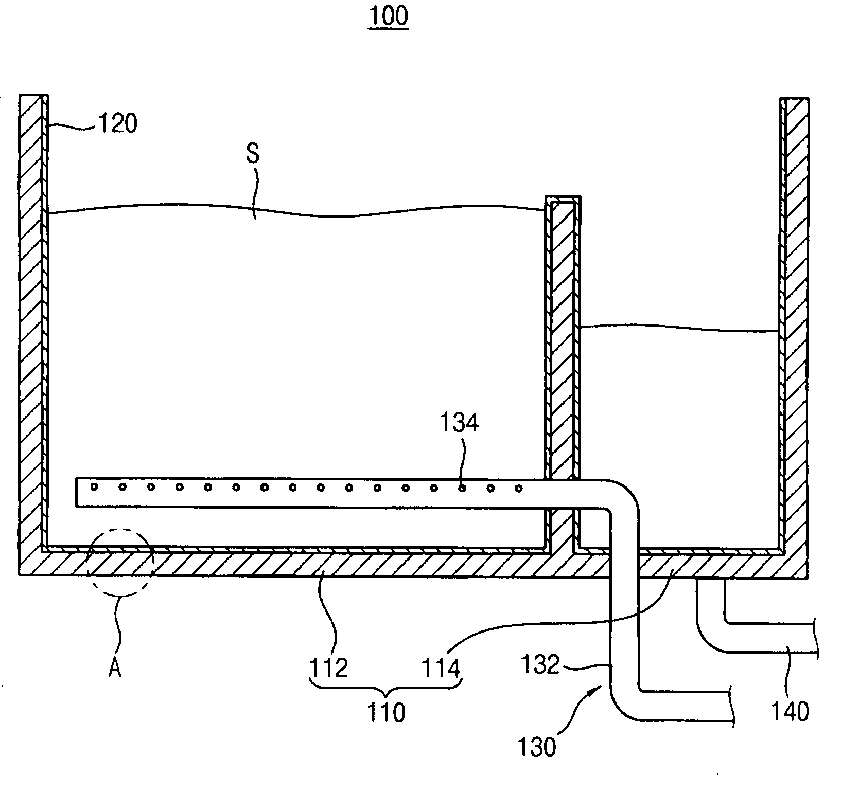
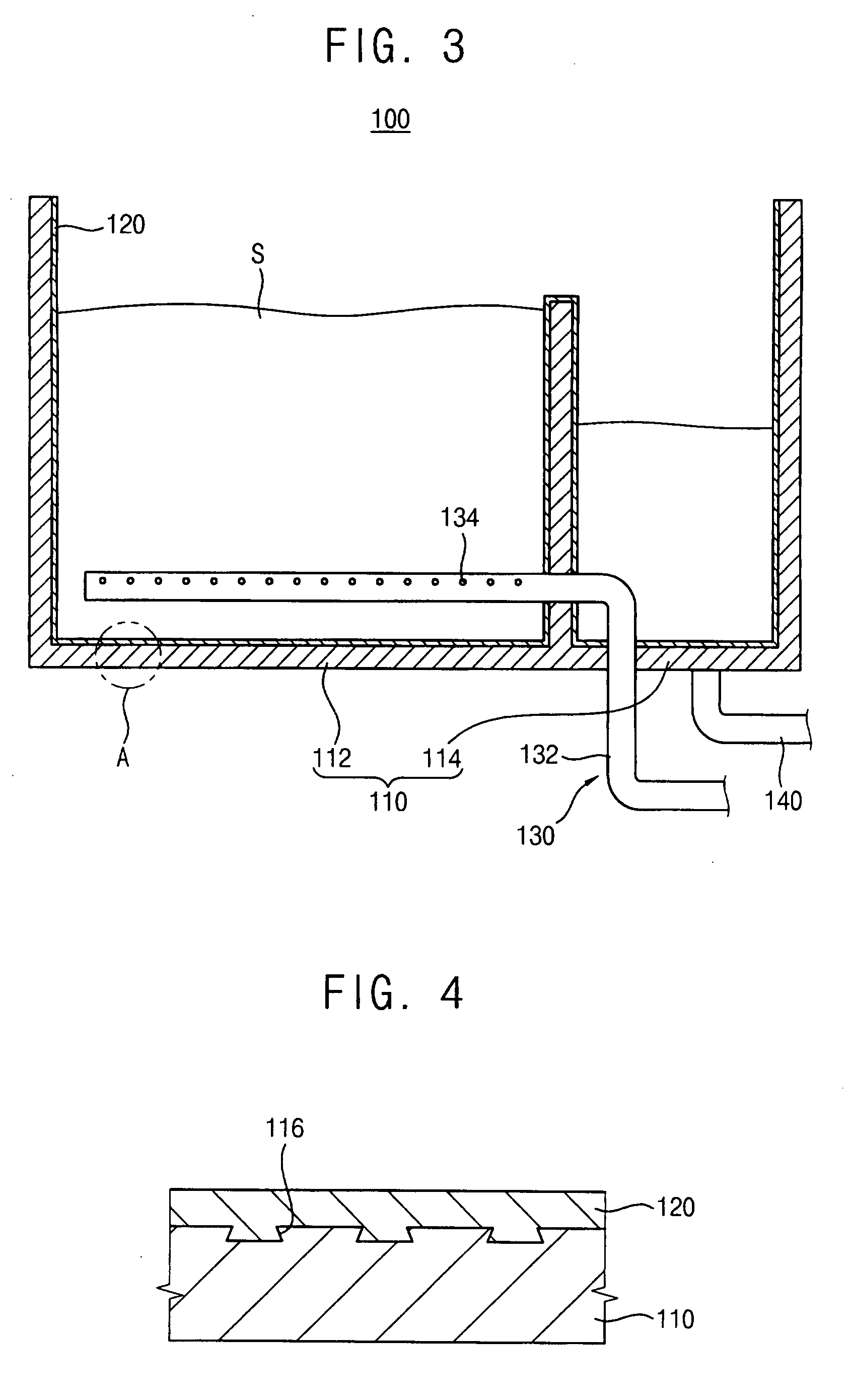
[0025]Reference will now be made in detail to example embodiments, examples of which are illustrated in the accompanying drawings. However, example embodiments are not limited to the embodiments illustrated hereinafter, and the embodiments herein are rather introduced to provide easy and complete understanding of the scope and spirit of example embodiments. In the drawings, the thicknesses of layers and regions are exaggerated for clarity.

[0026]It will be understood that when an element or layer is referred to as being “on,”“connected to” or “coupled to” another element or layer, it may be directly on, connected or coupled to the other element or layer or intervening elements or layers may be present. In contrast, when an element is referred to as being “directly on,”“directly connected to” or “directly coupled to” another element or layer, there are no intervening elements or layers present. Like reference numerals refer to like elements throughout. As used herein, the term “and / or...


PUM

PropertyMeasurementUnit
Temperatureaaaaaaaaaa
Diameteraaaaaaaaaa

Abstract

An apparatus for etching a semiconductor substrate may include a bath, a reaction preventing layer, and a nozzle. The bath may receive a chemical solution. Grooves may be formed at the inner wall of the bath. The reaction preventing layer may be formed on the inner wall and in the grooves of the bath to reduce or prevent a chemical reaction between the chemical solution and the bath. The nozzle may supply the chemical solution to the bath. In a method of etching a semiconductor substrate, the semiconductor substrate having trench structures and an insulation layer pattern may be prepared. The semiconductor substrate may then be dipped into the bath having the reaction preventing layer in which the chemical solution is received. The semiconductor substrate may be reacted with the chemical solution by blocking the chemical reaction between the chemical solution and the bath to etch the insulation layer pattern and the trench structure at a uniform rate.

Description

PRIORITY STATEMENT[0001]This application claims priority under 35 USC §119 to Korean Patent Application No. 2006-101159, filed on Oct. 18, 2006, in the Korean Intellectual Property Office (KIPO), the entire contents of which are herein incorporated by reference.BACKGROUND[0002]1. Field[0003]Example embodiments relate to an apparatus and a method of wet-etching a semiconductor substrate using a chemical.[0004]2. Description of Related Art[0005]In a process for forming a semiconductor device, a silicon nitride layer may be uniformly etched at a temperature of about 165° C. using a phosphoric acid (H3PO4) solution as an etching solution. When a wet etching process using a phosphoric acid solution is performed, a silicon oxide layer as well as the silicon nitride layer may be uniformly etched. The phosphoric acid solution may have a uniform etching selectivity within the range of the etching selectivity of the silicon nitride layer and the silicon oxide layer. For example, the etching s...

Claims


Application Information

Patent Timeline
IPC IPC(8): H01L21/461
CPCH01L21/31111H01L21/76224H01L21/67086H01L21/304H01L21/306
Inventor KIM, IN-GICHUNG, DAE-HYUKKANG, DAE-HYUK
Owner SAMSUNG ELECTRONICS CO LTD
Why Eureka
Try Eureka