Organic light emitting diode display and manufacturing method thereof

a technology of light-emitting diodes and organic light-emitting elements, which is applied in the direction of thermoelectric device junction materials, semiconductor devices, electrical apparatus, etc., can solve the problems of deterioration of the foregoing organic light-emitting elements, and achieve the effect of detecting defects easily

Active Publication Date: 2014-05-22
SAMSUNG DISPLAY CO LTD
View PDF7 Cites 11 Cited by
  • Summary
  • Abstract
  • Description
  • Claims
  • Application Information

AI Technical Summary

Benefits of technology

[0025]According to the exemplary embodiments, when the inspection wire is formed, it is possibl...

Problems solved by technology

The foregoing organic light emitting element may be deteriorated due to internal factors such as deterioration of the organic emission layer due to oxygen from indium tin oxide (ITO) used as electrode materials, deterioration due to reaction between interfaces of the organic material layers configuring the organic emission layer, and the like and may be deteriorated due to ...

Method used


Image

  • Organic light emitting diode display and manufacturing method thereof
  • Organic light emitting diode display and manufacturing method thereof
  • Organic light emitting diode display and manufacturing method thereof

Examples


Embodiment Construction

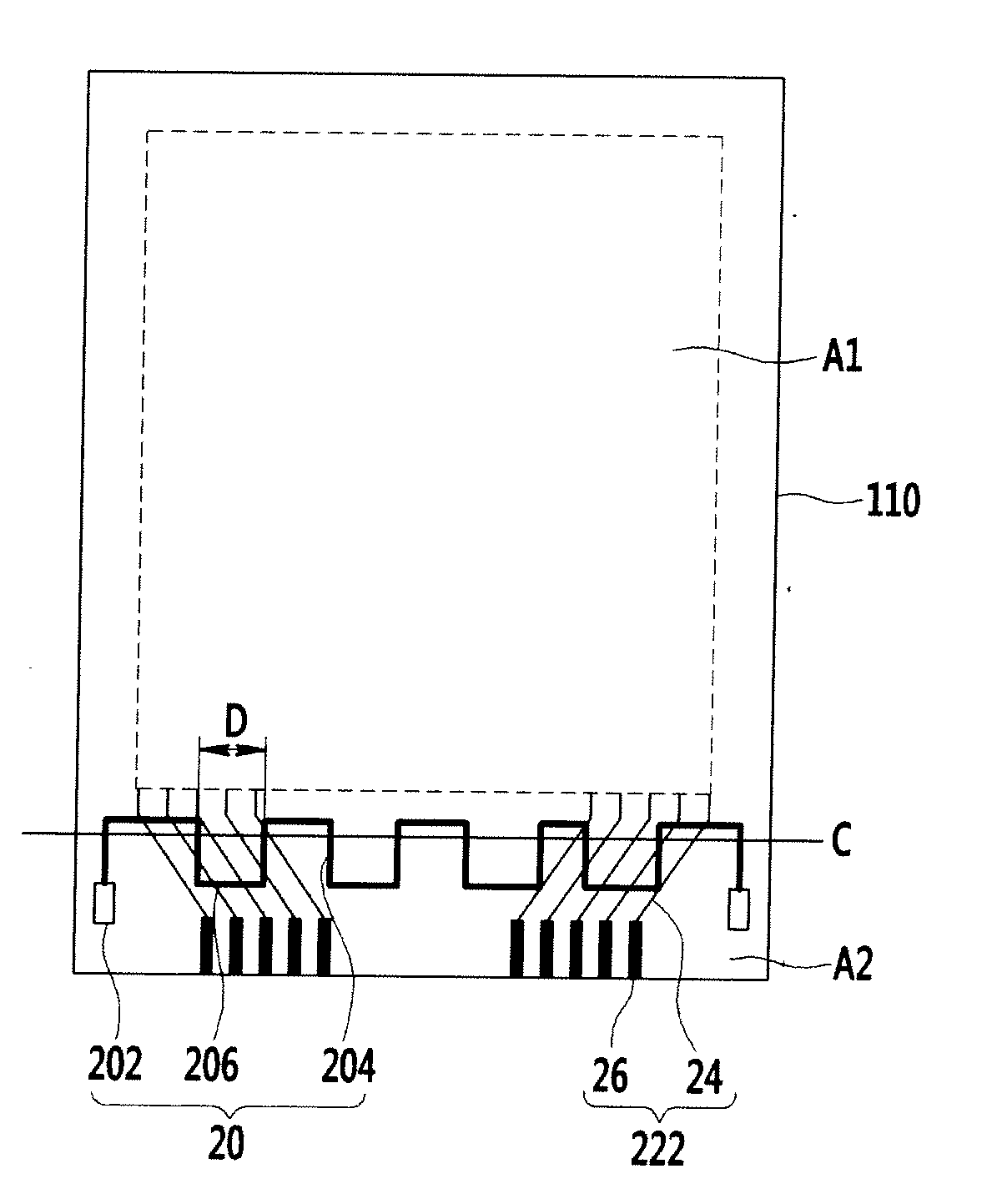
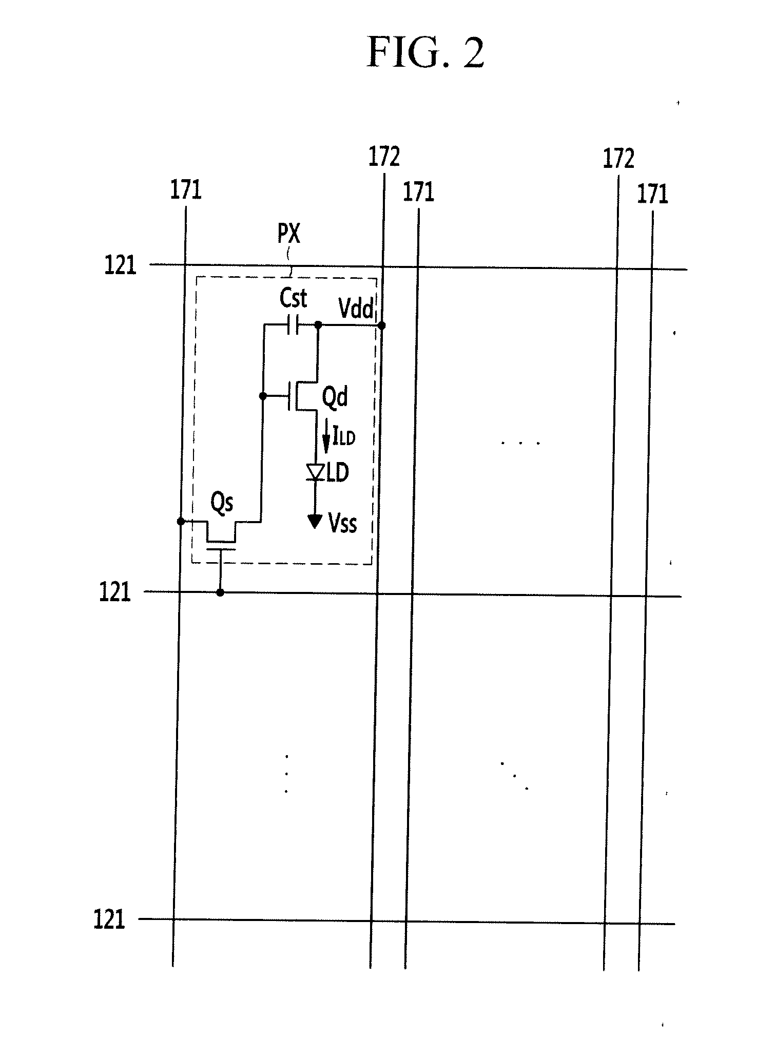
[0034]Embodiments of the present invention will be described more fully hereinafter with reference to the accompanying drawings, in which exemplary embodiments of the invention are shown by way of illustration. As those skilled in the art would realize, the described embodiments may be modified in various different ways, all without departing from the spirit or scope of the present invention and the invention should not be construed as being limited to the embodiments set forth herein.

[0035]The drawings and description are to be regarded as illustrative in nature and not restrictive. Like reference numerals designate like elements throughout the specification.

[0036]Further, a size and a thickness of each component illustrated in the drawings are arbitrarily shown for convenience of description and therefore the present invention is not necessarily limited thereto.

[0037]In the drawings, the thickness of layers, films, panels, regions, etc., are exaggerated for clarity. Further, in th...


PUM


Abstract

Disclosed is an organic light emitting diode display including: a substrate including a display area configured to display an image and a peripheral area surrounding the display area; a plurality of pad wires at the peripheral area of the substrate; and an inspection wire having a zigzag form on the plurality of pad wires.

Description

CROSS-REFERENCE TO RELATED APPLICATION[0001]This application claims priority to and the benefit of Korean Patent Application No. 10-2012-0131988 filed in the Korean Intellectual Property Office on Nov. 20, 2012, the entire contents of which are incorporated herein by reference.BACKGROUND[0002]1. Field[0003]The following description relates generally to an organic light emitting diode display and a manufacturing method thereof.[0004]2. Description of the Related Art[0005]An organic light emitting diode display includes organic light emitting elements, each of which includes a hole injection electrode, an organic emission layer, and an electron injection electrode. Each organic light emitting element emits light by energy generated when an exciton generated by a combination of electrons and holes in the organic emission layer falls from an excited state to a ground state. The organic light emitting diode display then generates a predetermined or preselected image using the light emiss...

Claims


Application Information

Patent Timeline
IPC IPC(8): H01L51/52H01L51/56
CPCH01L51/56H01L51/5253H10K59/131H10K71/70H10K50/841H10K71/00H10K50/844H10K2102/311
Inventor BAE, HAN-SUNGKWAK, WON-KYU
Owner SAMSUNG DISPLAY CO LTD
Why Eureka
Try Eureka