Method for continuous, in situ evaluation of entire wafers for macroscopic features during epitaxial growth

a technology of epitaxial growth and in situ evaluation, applied in the field of wafer evaluation, can solve the problems of surface roughness, interfere with the growth process, and surface haze can also form, and achieve the effects of reducing gallium desorption, enhancing gallium desorption, and improving non-uniformity in beam flux and substrate temperatur

Active Publication Date: 2008-05-01
RAYTHEON CO
View PDF12 Cites 2 Cited by
  • Summary
  • Abstract
  • Description
  • Claims
  • Application Information

AI Technical Summary

Benefits of technology

[0006]The inventors have recognized that due to non-uniformities in beam fluxes and substrate temperature, a technique is needed to monitor the entire wafer for substrate scratches and polish damage, surface haze, metallic accumulations such as gallium balls, pinholes in metal coatings, and other macroscopic defects. Further a technique is needed to monitor wafers that are rotated to improve non-uniformities in beam fluxes and substrate temperatures. With such a technique, large gallium balls could be periodically eliminated during growth by adjusting growth conditions. Thus, GaN growth can be performed with excess gallium on the surface without the consequences of large gallium balls affecting the growth. Further, knowledge of the location and the appearance of haze during a run may assist in diagnosing the problem with the growth conditions and / or substrate preparation. The location and concentration of pinholes or other macroscopic defects also need to be characterized. Furthermore the relative temperature uniformity across the wafer can be determined as cold spots (reduced gallium desorption) lead to gallium balls and hot spots (enhanced gallium desorption) lead to haze.

Problems solved by technology

If the gallium balls become too large, however, they will back-dissolve the substrate surface, resulting in surface roughening and will also interfere with the growth process.
Surface haze can also form if the substrate surface is not atomically clean prior to growth since the surface crystallinity is disrupted leading to a rough surface.
Another issue encountered in epitaxial film growth on substrates requiring a backside coating for effective and uniform heating is the presence of pinholes in the coating.
The occurrence of pinholes leads to substrate temperature non-uniformities in the vicinity of the pinhole and can perturb pyrometer readings.
However, the inventors have recognized that the technique has important limitations.
This limitation becomes more serious with increasing wafer diameter not only due to the limited sample area but also the increased non-uniformity of film fluxes and substrate temperatures over larger areas.

Method used


Image

  • Method for continuous, in situ evaluation of entire wafers for macroscopic features during epitaxial growth
  • Method for continuous, in situ evaluation of entire wafers for macroscopic features during epitaxial growth
  • Method for continuous, in situ evaluation of entire wafers for macroscopic features during epitaxial growth

Examples


Embodiment Construction

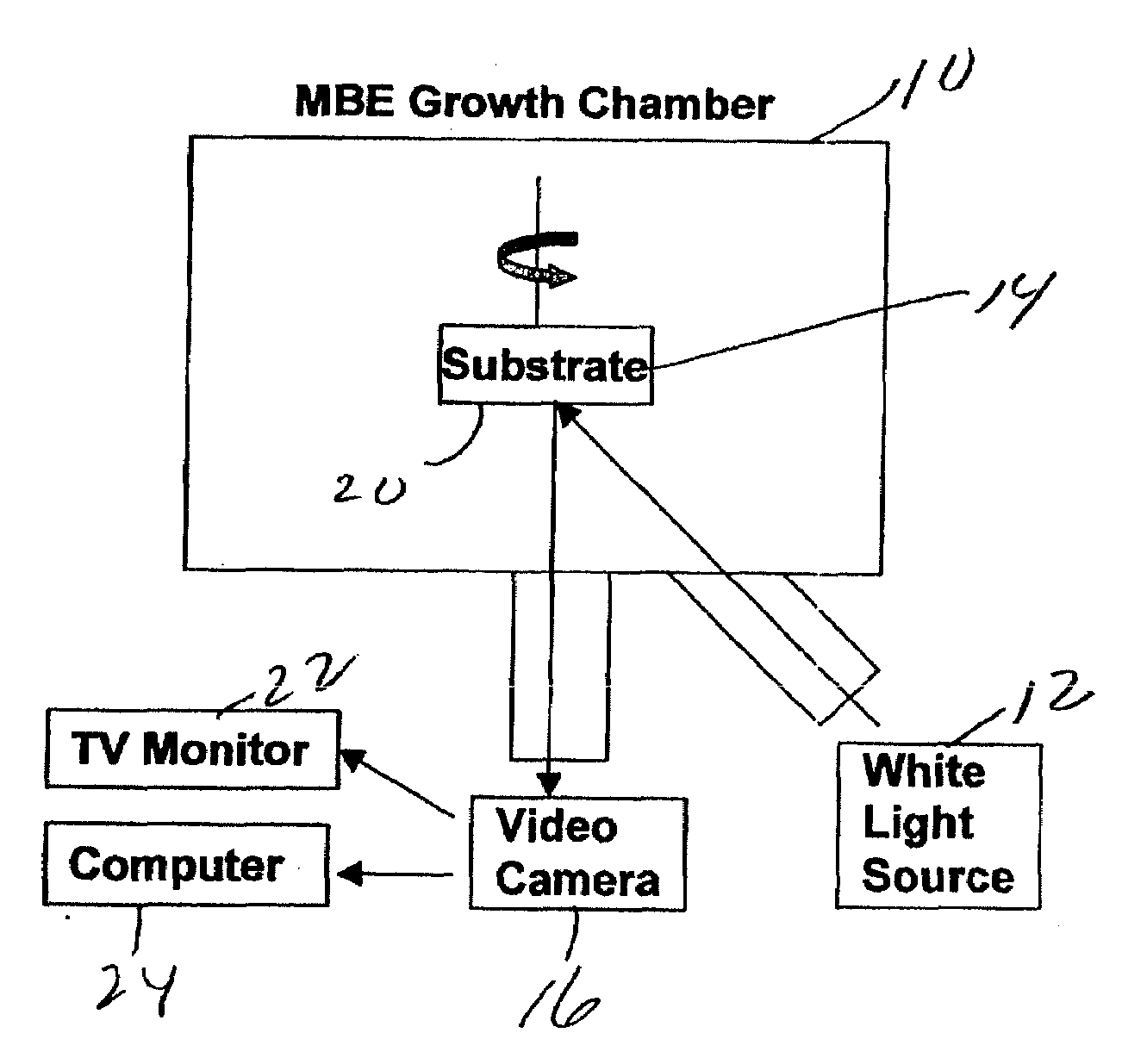
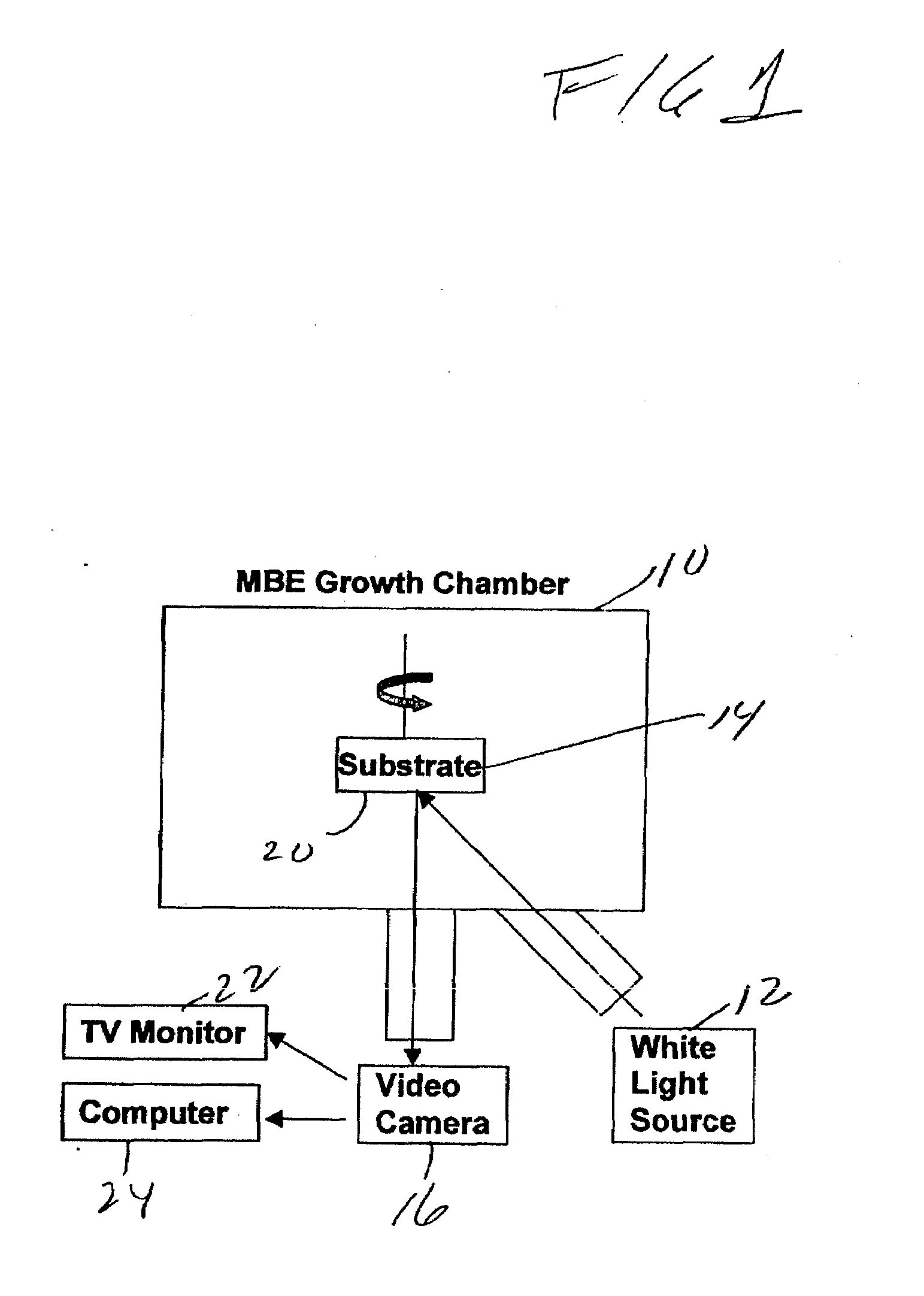
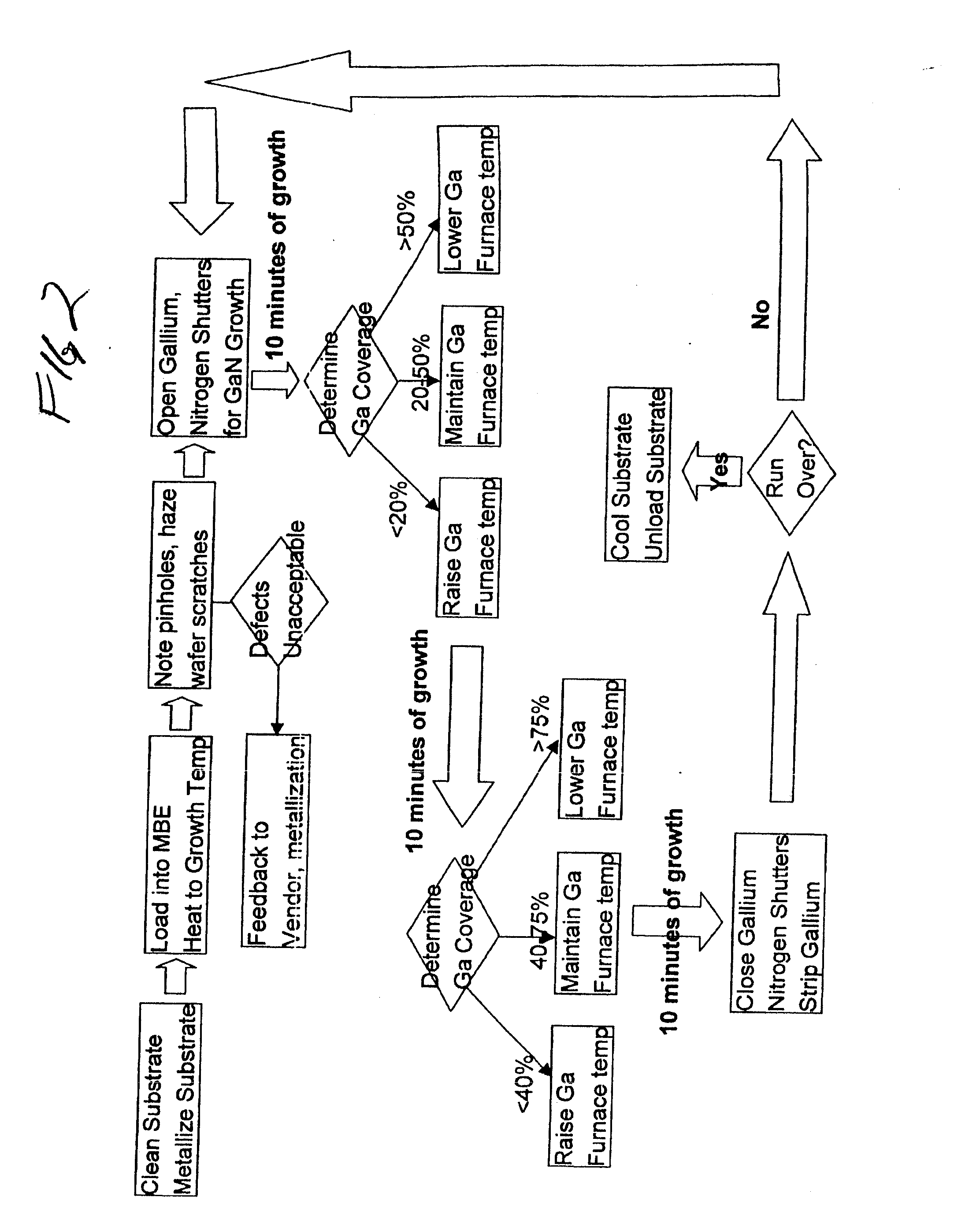
[0017]Referring now to FIG. 1, a schematic of the invention incorporated on a molecular beam epitaxy (MBE) apparatus 10, here manufactured by VEECO model Gen 20 MBE is shown. Here white light source 12 (i.e., light over the entire visible spectrum) mounted to one flange of the MBE apparatus 10 is used to illuminate the entire growth surface of a wafer 14 or substrate, here for example, a 3-inch SiC wafer. A video camera 16 is mounted on another flange with nonspecular geometry to the light source 12. The viewing angle of the camera 16 is different from the angle of reflection of the axis of the beam of the light source 12 from the surface 20 of the wafer. The camera 16 is connected to a TV monitor 22 for viewing of the entire surface of the wafer and a computer 24 to capture images generated by the camera 16. When the growth surface 20 of wafer 14 is smooth the light specularly reflects off the surface 20 and is not significantly detected by the camera 16 resulting in a dark wafer i...


PUM

PropertyMeasurementUnit
non-specular angleaaaaaaaaaa
temperatureaaaaaaaaaa
crystallinityaaaaaaaaaa

Abstract

Apparatus and method for growing and observing the growth of epitaxial layers on a wafer. The apparatus includes: epitaxial growth apparatus; a source of light mounted to illuminate an entire surface of the wafer in the apparatus during growth of the epitaxial layer on the entire surface of the wafer; and apparatus for observing scattering of the light from the entire surface of the wafer during growth of the epitaxial layer on the entire surface of the wafer. The method includes growing the epitaxial layer on a surface of the wafer and observing scattering of the light from the entire surface of the wafer during growth of the epitaxial layer on the entire surface of the wafer. The growing process is varied in accordance with the observation. With an epitaxial layer of gallium nitride (GaN) the entire surface of the wafer is observed for balls of gallium.

Description

TECHNICAL FIELD[0001]This invention relates generally to wafer evaluation and more particularly to methods for continuous, in situ evaluation of entire wafers for macroscopic features during epitaxial growth.BACKGROUND AND SUMMARY[0002]As is known in the art, epitaxial growth of semiconductor films, such as performed by molecular beam epitaxy (MBE) or metalorganic chemical vapor deposition (MOCVD) depends critically on the magnitudes and uniformities of reactant atoms on the substrate surface as well as the temperature and its uniformity across the substrate. In the specific example of plasma MBE growth of GaN, gallium atoms are evaporated onto the substrate surface in the presence of reactive nitrogen provided by a plasma source. The highest quality films are obtained when the net gallium beam flux (incoming gallium flux minus the gallium desorption rate) exceeds the reactive nitrogen beam flux resulting in a gallium adlayer on the growing surface. The gallium desorption rate from ...

Claims


Application Information

Patent Timeline
Patent Type & Authority Applications(United States)
IPC IPC(8): C30B15/26C30B15/30C30B11/00
CPCC30B23/02C30B35/00G01N21/4738G01N21/8422Y10T117/1004G01N21/951G01N2021/8416Y10T117/1012Y10T117/1008G01N21/9501
Inventor HOKE, WILLIAM E.KENNEDY, THEODORE D.
Owner RAYTHEON CO
Why Eureka
Try Eureka