Thermal-type infrared imaging device and operation method thereof

a technology of infrared imaging and thermal imaging, which is applied in the field of imaging devices, can solve the problems of loss of temperature information, inability to output appropriate temperature information, and difficulty in achieving both high temperature resolution and wide temperature measurement range at the same time, and achieves the effect of wide temperature measurement range and high temperature resolution

Active Publication Date: 2008-05-01
NEC CORP
View PDF4 Cites 11 Cited by
  • Summary
  • Abstract
  • Description
  • Claims
  • Application Information

AI Technical Summary

Benefits of technology

[0012]In view of the foregoing, it is a main object of the present invention to provide an imaging device, particularly, a thermal-type infrared imaging device and its operation method that can achieve both a high temperature resolution and a wide temperature measurement range at the same time without requiring the user to change the setting.
[0021]As described above, the signal processing unit sets the sensitivity of each pixel according to a predetermined pattern in synchronization with the switching operation for reading the signal of the infrared ray detection device of the pixel and classifies a plurality of pixels into a plurality of types of pixels having different sensitivities. The thermal-type infrared imaging device having such configuration can achieve a high temperature resolution and a wide temperature measurement range at the same time without requiring the user to change the sensitivity setting even when a subject with a wide temperature range is imaged.
[0027]The thermal-type infrared imaging device and its operation method of the present invention can achieve a high temperature resolution and a wide temperature measurement range at the same time without requiring the user to change the sensitivity setting.
[0028]The reason is that the present invention provides a thermal-type infrared imaging device at least comprising an infrared ray detection unit in which pixels, each of which includes an infrared ray detection device, are arranged in a two-dimensional matrix; and a signal processing unit that processes signals from the infrared ray detection unit. The signal processing unit sets the sensitivity of each of the pixels according to a predetermined pattern in synchronization with the switching operation for reading the signal of the infrared ray detection device of each pixel and classifies a plurality of pixels into a plurality of types of pixels having different sensitivities, such as pixels for which high sensitivity (narrow temperature measurement range—high temperature resolution) is set and pixels for which low sensitivity (wide temperature measurement range—low temperature resolution) is set. Therefore, the thermal-type infrared imaging device can achieve a fine temperature resolution near the room temperature and, at the same time, a temperature measurement range wide enough for measuring even a high-temperature subject, without requiring the user to change the sensitivity setting.

Problems solved by technology

The problem here is that, when the temperature of a subject exceeds the temperature measurement range that is set, the image output becomes saturated and all temperatures equal to or higher than a predetermined value are output as a signal of the upper limit temperature, resulting in a loss of the temperature information.
On the other hand, when the temperature distribution of a subject is narrow compared to a sensitivity that has been set, a sufficient temperature resolution is not obtained and, so, appropriate temperature information cannot be output.
This problem requires the user to change the sensitivity in order to output an appropriate infrared ray image when the sensitivity setting differs much from a right setting for the subject temperature.
However, because there is a tradeoff between the temperature resolution and the temperature measurement range in a predetermined output voltage range as described above, it is difficult to achieve both a high temperature resolution and a wide temperature measurement range at the same time.
Thus, in the case with the fire site given above, for instance, the thermal-type infrared imaging device the user is required to change the sensitivity setting of according to the situation, making the operation complex.
Failure to do so results in the problem that the temperature information is lost or appropriate temperature information cannot be obtained.

Method used


Image

  • Thermal-type infrared imaging device and operation method thereof
  • Thermal-type infrared imaging device and operation method thereof
  • Thermal-type infrared imaging device and operation method thereof

Examples


first exemplary embodiment

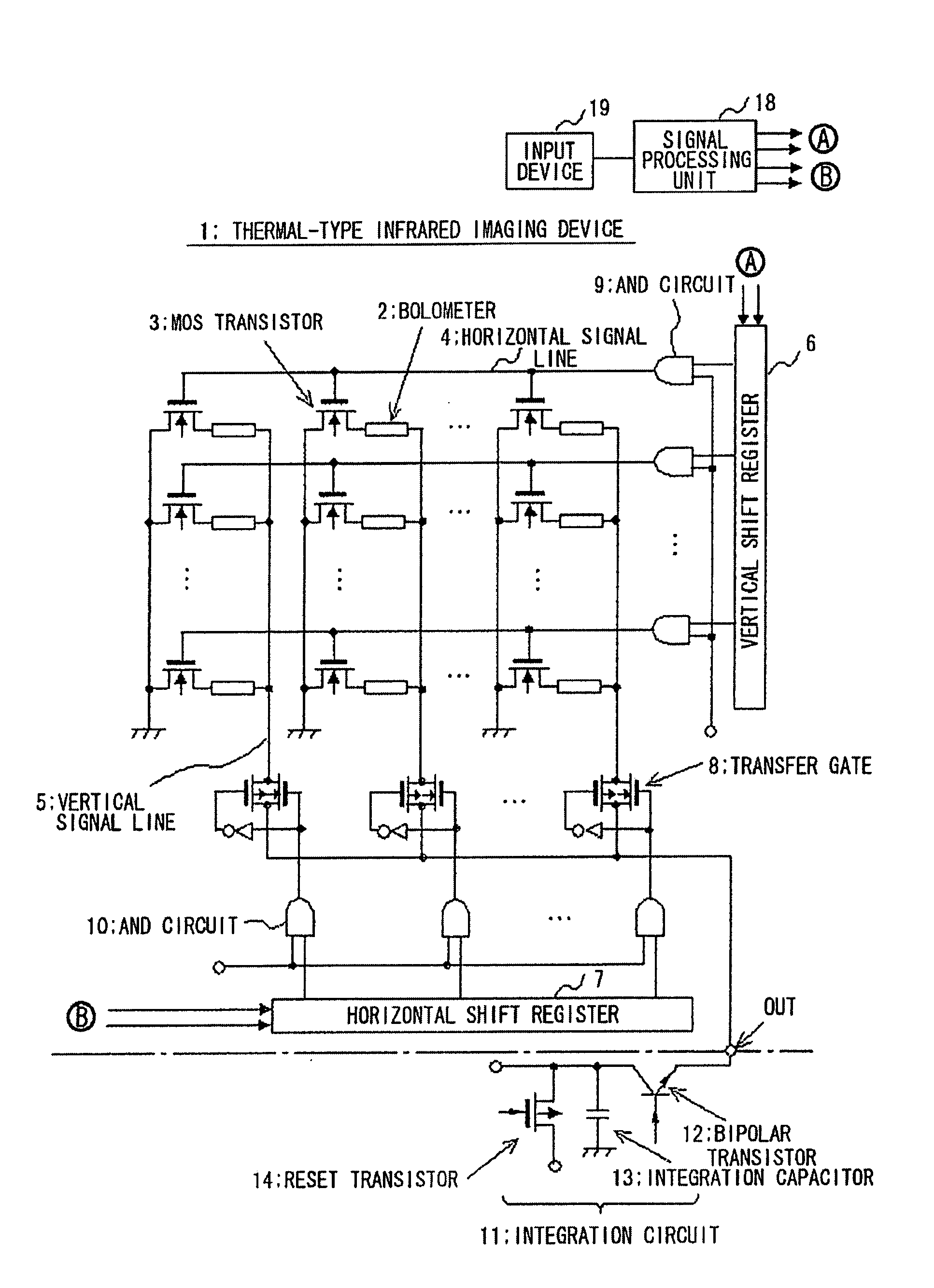
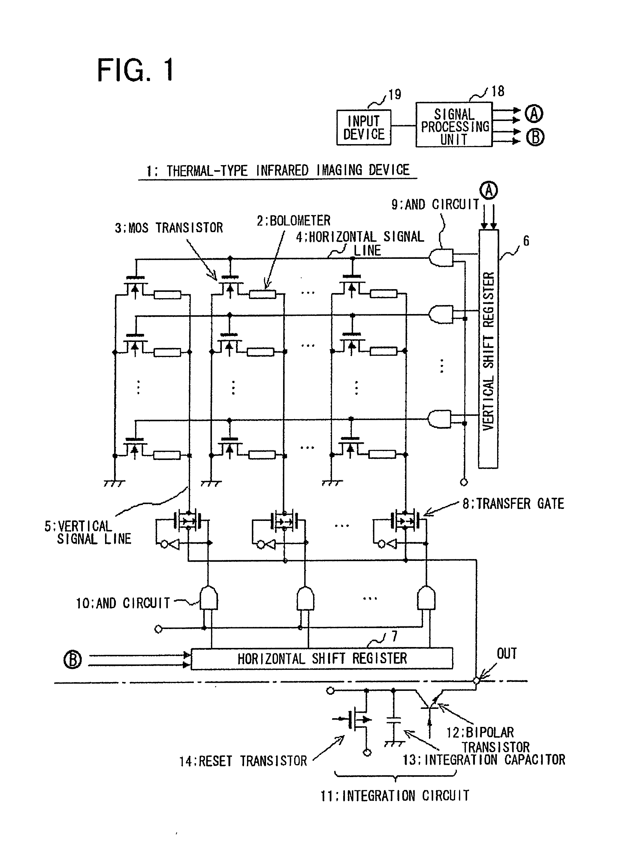
[0039]To describe the preferred exemplary embodiment of the present invention more in detail, a thermal-type infrared imaging device in a first exemplary embodiment of the present invention and its operation method will be described with reference to FIG. 1 to FIG. 5. FIG. 1 is a circuit diagram showing the configuration of the thermal-type infrared imaging device in this exemplary embodiment, and FIG. 2 to FIG. 4 are diagrams showing the arrangement of pixels in the thermal-type infrared imaging device in this exemplary embodiment. FIG. 5 is a flowchart showing the operation of the thermal-type infrared imaging device in this exemplary embodiment.

[0040]As shown in FIG. 1, a thermal-type infrared imaging device 1 comprises an infrared ray detection unit composed of multiple pixels arranged two dimensionally, a signal processing unit that processes signals from the infrared ray detection unit, and so on. The signal processing unit comprises internal circuits built in the substrate an...

second exemplary embodiment

[0051]Next, a thermal-type infrared imaging device in a second exemplary embodiment of the present invention and its operation method will be described with reference to FIG. 6. FIG. 6 is a diagram showing the arrangement of pixels in the thermal-type infrared imaging device in this exemplary embodiment.

[0052]In the first exemplary embodiment described above, the multiple devices arranged in a two-dimensional matrix are classified into high-sensitivity pixels 15 and low-sensitivity pixels 16. In this exemplary embodiment, the multiple devices arranged two-dimensionally are classified into three types as shown in FIG. 6, that is, high-sensitivity pixels (H) 15, low-sensitivity pixels (L) 16, and intermediate-sensitivity pixels 17 (pixel indicated by M) that has a sensitivity lying between the high sensitivity and the low sensitivity. Those three types of pixels are used to achieve three types of sensitivities at the same time Those three types of sensitivities enable a subject to be ...


PUM


Abstract

Thermal-type infrared imaging device comprises an infrared ray detection unit in which pixels, each of which includes a bolometer, are arranged two-dimensionally; and a signal processing unit that sequentially reads signal of each bolometer in synchronization with switching operation of a horizontal shift register and a vertical shift register, integrates the read signal using an integration circuit, and outputs the integrated signal. The signal processing unit is configured so that it can set a sensitivity (for example, voltage applied to bolometer, capacitance of a capacitor in the integration circuit, and / or period of time for integrating the signal) for each pixel according to a predetermined pattern in synchronization with switching operation for classifying a plurality of pixels into a plurality of types of pixels for which different sensitivities are set, for example, high-sensitivity pixels 15 with a narrow temperature measurement range and a high temperature resolution and low-sensitivity pixels 16 with a wider temperature measurement range and a lower temperature resolution than those of the high-sensitivity pixels 15.

Description

REFERENCE TO RELATED APPLICATION[0001]This application is based upon and claims the benefit of the priority of Japanese patent application No. 2006-295681, filed on Oct. 31, 2006, the disclosure of which is incorporated herein in its entirety by reference thereto.FIELD OF THE INVENTION[0002]The present invention relates to an imaging device, particularly to a thermal-type infrared imaging device and operation method thereof, and more particularly to a thermal-type infrared imaging device, which uses bolometers as infrared ray (IR ray) detection devices, and operation method thereof.BACKGROUND OF THE INVENTION[0003]A thermal-type infrared imaging device is known that uses bolometers as detectors for imaging the temperature distribution of a subject. A bolometer is a device that detects an infrared ray through the operation on the phenomenon that the resistance value of a resistor varies when an infrared ray enters the resistor. The thermal-type infrared imaging device has a two-dimen...

Claims


Application Information

Patent Timeline
Patent Type & Authority Applications(United States)
IPC IPC(8): H01L27/16
CPCG01J1/44G01J5/22H04N5/35563H04N5/335H04N5/33H04N25/00H04N25/585
Inventor TAKEMURA, KOUJIEGASHIRA, KAZUYUKITANAKA, YUTAKA
Owner NEC CORP
Why Eureka
Try Eureka