
Apparatus and method for determining on die termination modes in memory device

a technology of memory devices and termination modes, applied in the direction of pulse techniques, digital storage, reliability increasing modifications, etc., can solve the problems of difficult verification of the enablement of dynamic odt mode, signal reflection more significantly degrades si in memory systems having high-speed operations, etc., and achieves the effect of more flexibility

Inactive Publication Date: 2008-05-01
SAMSUNG ELECTRONICS CO LTD
View PDF4 Cites 15 Cited by
  • Summary
  • Abstract
  • Description
  • Claims
  • Application Information

AI Technical Summary

Benefits of technology

[0012]Accordingly, the present invention determines enablement of the normal ODT mode and the dynamic ODT mode in a semiconductor memory device with more flexibility.
[0023]By using such signals and such logic elements, the normal ODT mode and the dynamic ODT mode are enabled with more flexibility in the present invention.

Problems solved by technology

In particular, signal reflection more significantly degrades SI in a memory system having high-speed operations.
However, verification of enablement of the dynamic ODT mode is difficult in the prior art because the dynamic ODT mode is enabled while the normal ODT mode is also enabled.

Method used


Image

  • Apparatus and method for determining on die termination modes in memory device
  • Apparatus and method for determining on die termination modes in memory device
  • Apparatus and method for determining on die termination modes in memory device

Examples


Embodiment Construction

[0033]The present invention will now be described more fully hereinafter with reference to the accompanying drawings, in which preferred embodiments of the invention are shown. This invention may, however, be embodied in many different forms and should not be construed as being limited to the embodiments set forth herein. Rather, these embodiments are provided so that this disclosure will be thorough and complete, and will fully convey the scope of the invention to one skilled in the art.

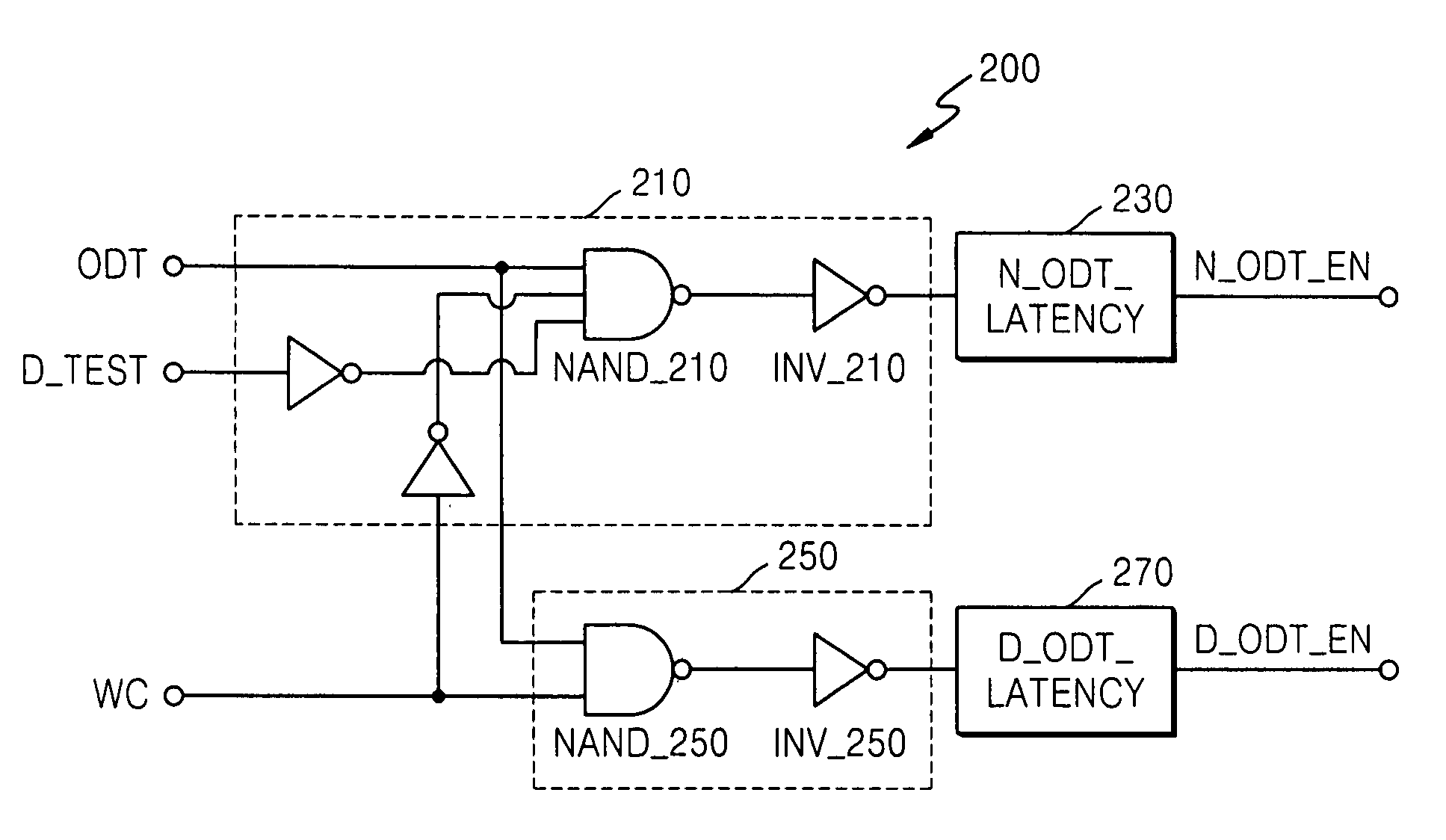
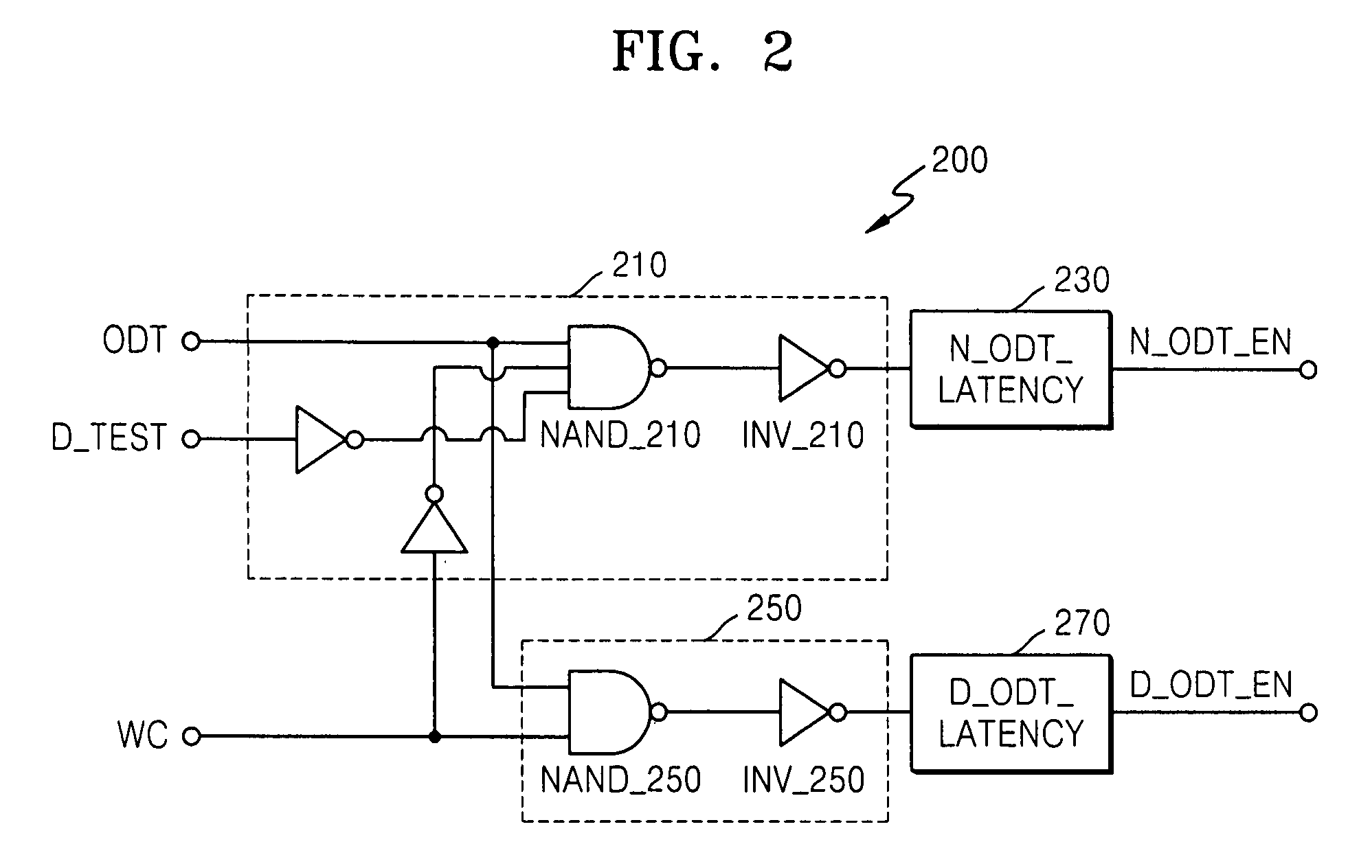
[0034]FIG. 2 is a block diagram of an on die termination (ODT) mode test apparatus 200 according to an embodiment of the present invention. Referring to FIG. 2, the ODT mode test apparatus 200 includes a first mode determining unit 210, a normal ODT latency unit N_ODT_LATENCY 230, a second mode determining unit 250, and a dynamic ODT latency unit D_ODT_LATENCY 270.

[0035]The first mode determining unit 210 determines whether or not a normal ODT mode is enabled in response to a dynamic ODT mode test s...


PUM


Abstract

For determining an on die termination (ODT) mode in a semiconductor memory device, a first mode determining unit determines whether or not a normal ODT mode is enabled from performing a logic operation on a first set of signals. A second mode determining unit determines whether or not a dynamic ODT mode test is enabled from performing a logic operation on a second set of signals. One of the normal and dynamic ODT modes is enabled with more flexibility.

Description

BACKGROUND OF THE INVENTION[0001]This application claims priority under 35 USC §119 to Korean Patent Application No. 2006-105039, filed on Oct. 27, 2006 in the Korean Intellectual Property Office, the disclosure of which is incorporated herein in its entirety by reference.[0002]1. Field of the Invention[0003]The present invention relates generally to on die termination in semiconductor memory devices, and more particularly, to determining on die termination modes in a semiconductor memory device.[0004]2. Background of the Invention[0005]On die termination (ODT) is used for improving signal integrity (SI) by minimizing signal reflection at an interface between a system and a memory device. In particular, signal reflection more significantly degrades SI in a memory system having high-speed operations. For suppressing signal reflection, a transmission line for signal transmission between the system and the memory device is terminated at a termination register (RTT).[0006]Conventionally...

Claims


Application Information

Patent Timeline
Patent Type & Authority Applications(United States)
IPC IPC(8): H03K17/16
CPCG11C7/1048G11C29/02H03K19/0005G11C29/028G11C29/025G11C29/00G11C7/10
Inventor CHOI, SUNG-HOOH, REUM
Owner SAMSUNG ELECTRONICS CO LTD
Learn More