Semiconductor memory device having write data through function

a memory device and function technology, applied in the direction of information storage, static storage, digital storage, etc., can solve the problems of increasing the load of designing rams, short time period during which write data is output and held on a data bus connecting to the semiconductor memory device (ram) on the chip (cpu or controller) side, and extremely small timing margin of chip design. to achieve the effect of facilitating the timing design of a semiconductor memory devi

Active Publication Date: 2008-05-01
RENESAS ELECTRONICS CORP
View PDF1 Cites 0 Cited by
  • Summary
  • Abstract
  • Description
  • Claims
  • Application Information

AI Technical Summary

Benefits of technology

[0032]The present invention facilitates the timing design of a semiconductor memory device including a Write Data Through mode or function and of a chip connected to the semiconductor memory device, by a configuration that equalizes access time in a read operation with access time in a write operation.

Problems solved by technology

That is, the time period during which write data is output and held on a data bus connecting to the semiconductor memory device (RAM) on the chip (CPU or controller) side is extremely short in a Write Data Through operation.
Consequently, timing margin of chip design is extremely small.
Accordingly, the load of designing RAMs increases.

Method used


Image

  • Semiconductor memory device having write data through function
  • Semiconductor memory device having write data through function
  • Semiconductor memory device having write data through function

Examples


Embodiment Construction

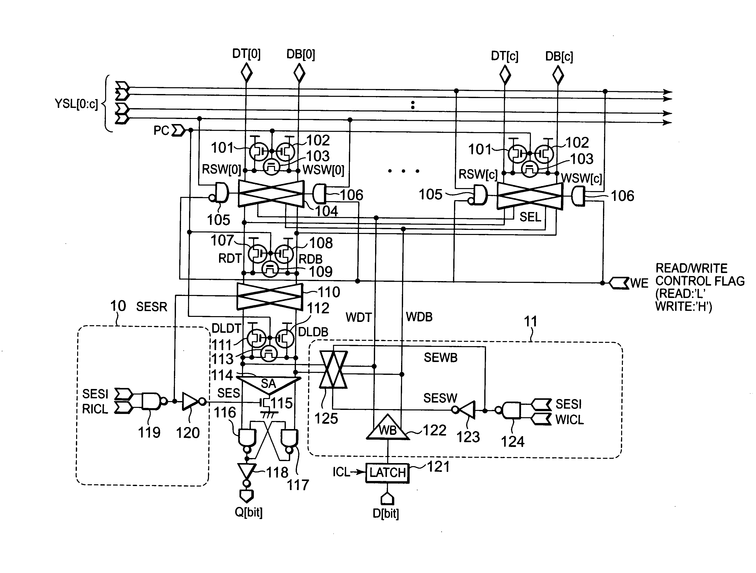
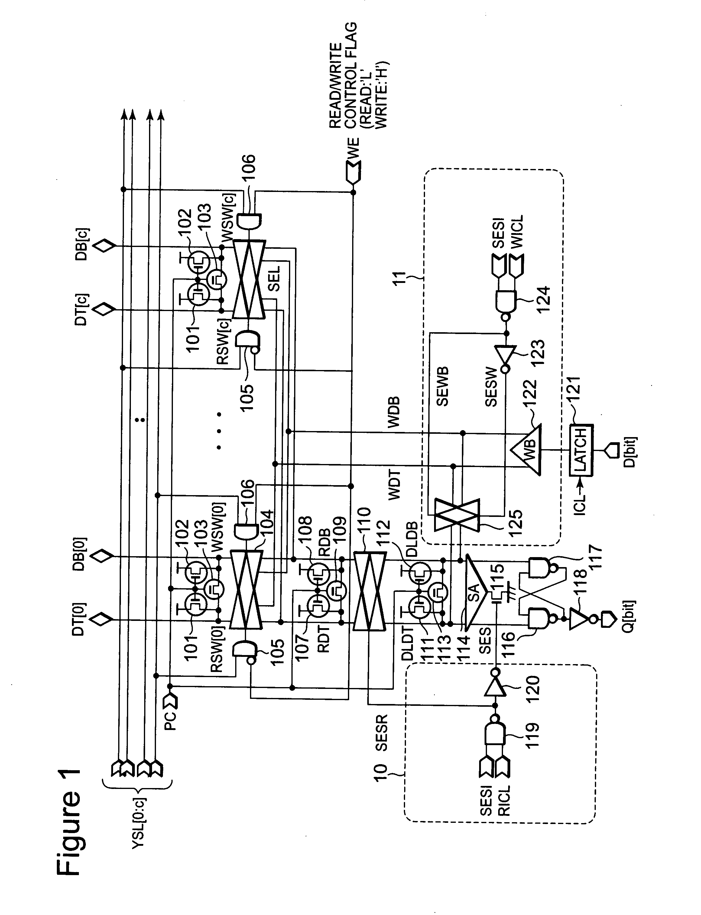
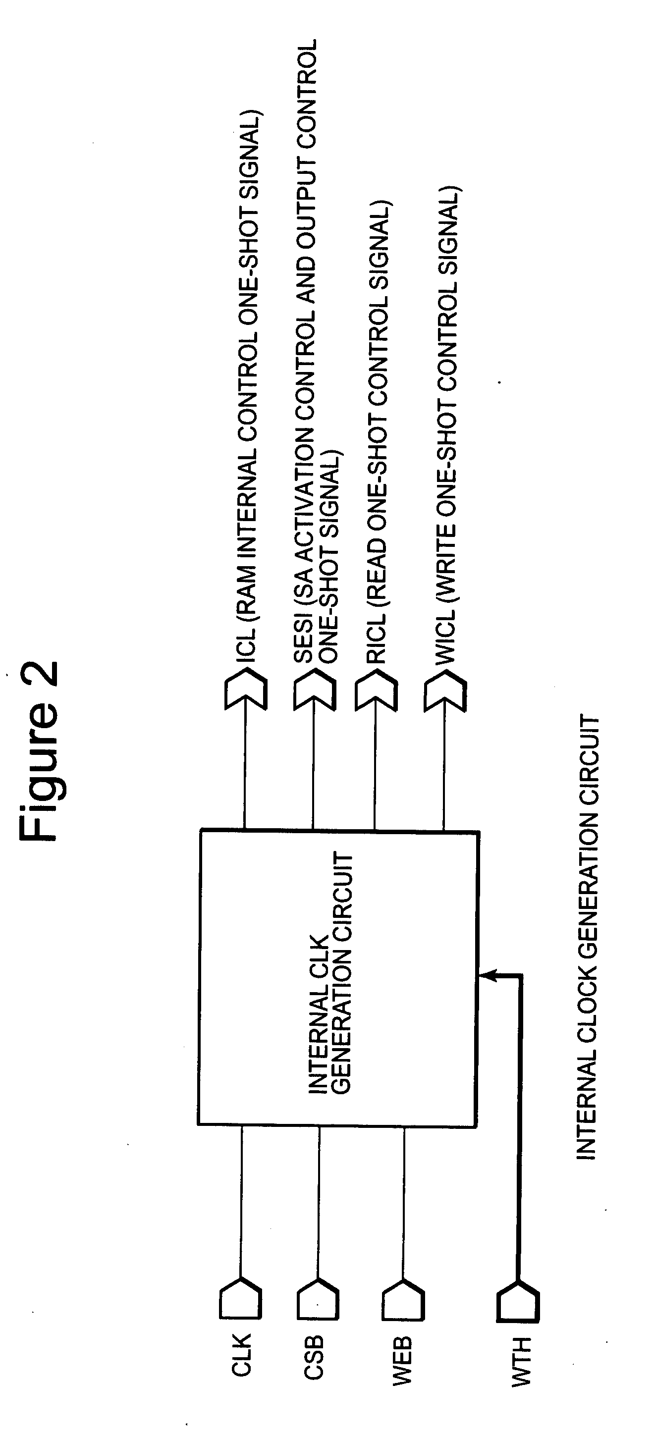
[0042]According to the present invention, a switch (125) is provided that turns on or off connection between a write data line pair (WDT / WDB) to which an output pair of a write buffer (122) is connected and a data line pair (DLDT / DLDB) to which a sense amplifier (114) is connected. A circuit (see FIG. 2) that generates a one-shot pulse signal (WICL) which is activated at a write operation when a Write Data Through specification is enabled is provided. Circuits (123, 124) are provided that receive WICL and a sense amplifier activation signal (SESI) and, when both of the signals are active, turn on the switch (125). Thus, the data hold time tOHW in a write operation when the Write Data Through specification is enabled can be made approximately equal to the data hold time tOHR in a read operation.

[0043]By providing a mechanism (switching based on the signal level at the WTH terminal shown in FIG. 2 or switching measures using a fuse or the like) that enables selection between two diffe...


PUM


Abstract

A semiconductor memory device includes a switch that turns on or off connection between a write data line pair which is an output of a write buffer and read data line pair. For a Write Data Through function, the switch is turned on in response to an activated one-shot pulse and a sense amplifier activation signal, thereby approximately equalizing data hold time tOHW in the Write Data Through function and data hold time tOHR in a read operation.

Description

BACKGROUND OF THE INVENTION[0001]1. Field of the Invention[0002]The present invention relates to a semiconductor memory device and, in particular, to a semiconductor memory device including a Write Data Through function which outputs input write data in a write operation.[0003]2. Description of Related Art[0004]FIG. 6 shows an example of a typical configuration of a semiconductor memory device. Digit lines and a portion surrounding an input and output circuits in the semiconductor memory device are mainly shown in FIG. 6. Referring to FIG. 6, PMOS transistors 301 and 302 having sources commonly connected to a power supply, gates commonly connected to a precharge control signal PC, and drains connected to digit lines DT and DB, respectively, are circuits that precharge the digit line pair DT / DB. A PMOS transistor 303 connected between the digit lines DT and DB and having a gate connected to the precharge control signal PC is a circuit that equalizes the digit line pair DT / DB. Each of...

Claims


Application Information

Patent Timeline
Patent Type & Authority Applications(United States)
IPC IPC(8): G11C7/00
CPCG11C7/1051G11C7/1069G11C7/22G11C7/1096G11C7/1078
Inventor KOGA, TOSHIRO
Owner RENESAS ELECTRONICS CORP
Why Eureka
Try Eureka