Display control semiconductor integrated circuit

a technology of integrated circuits and semiconductors, applied in the field of display controllers, can solve the problems of difficult timing design of peripheral circuits of memories, deterioration of yield, and easy defects, and achieve the effect of improving yield

Active Publication Date: 2011-11-29
SYNAPTICS JAPAN GK
View PDF8 Cites 1 Cited by
  • Summary
  • Abstract
  • Description
  • Claims
  • Application Information

AI Technical Summary

Benefits of technology

[0007]The inventors of the present invention tried to increase packing density of a built-in RAM by employing microfabrication process in order to reduce the chip size of a liquid crystal controller / driver and lower the chip cost. However, it was found that when the packing density of a built-in RAM is increased, a defect occurs more easily and a problem of deterioration in the yield due to defects in the RAM arises.
[0011]An object of the present invention is to repair a defective bit included in a RAM without increasing the occupation area so much in a display control semiconductor integrated circuit such as a liquid crystal controller / driver having therein a RAM that stores display data, thereby enabling the yield to be improved.
[0019]By the above-described means, it is unnecessary to construct, as separate circuits, a control circuit for selecting a normal memory row or column and a control circuit for selecting a spare memory row or column to be replaced with a defective bit, and it facilitates timing design of peripheral circuits of the memory.
[0023]According to the present invention, in a display control semiconductor integrated circuit such as a liquid crystal controller / driver having therein a RAM for storing display data, a defective bit included in the RAM is repaired and the yield can be improved without significantly increasing the occupation area.

Problems solved by technology

However, it was found that when the packing density of a built-in RAM is increased, a defect occurs more easily and a problem of deterioration in the yield due to defects in the RAM arises.
Since operation characteristics such as reading speed at the time of accessing a row or column in a normal memory and those at the time of accessing a row or column in a spare memory are different from each other, there is a problem such that designing of timings in peripheral circuits of the memories is difficult.
Consequently, when the memory defect repairing technique of the general RAM is applied directly to the liquid crystal controller / driver, there is a problem such that the occupation area of the redundancy circuit and the wiring becomes large, and it causes disturbance of reduction in the chip size.

Method used


Image

  • Display control semiconductor integrated circuit
  • Display control semiconductor integrated circuit
  • Display control semiconductor integrated circuit

Examples


Embodiment Construction

[0034]Preferred embodiments of the present invention will be described hereinbelow with reference to the drawings.

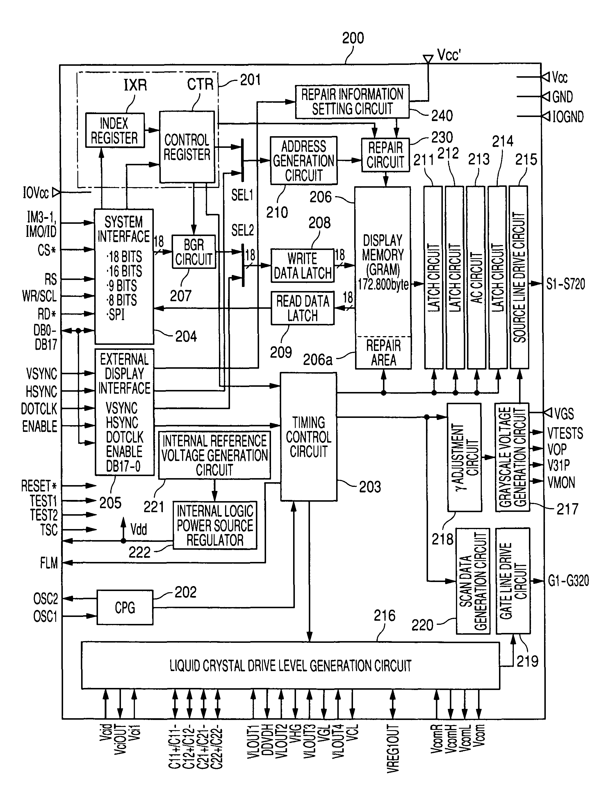
[0035]FIG. 1 is a block diagram showing an embodiment of a liquid crystal controller / driver 200 having therein a RAM and a repair circuit. The liquid crystal controller / driver 200 has therein a RAM (hereinbelow, called a display memory) as a memory for storing data to be graphic-displayed on a dot-matrix-type liquid crystal display panel. The liquid crystal controller / driver 200 is constructed as a semiconductor integrated circuit on a single semiconductor substrate together with a write circuit, a read circuit, and a driver for outputting a drive signal of a liquid crystal display panel.

[0036]The liquid crystal controller / driver 200 of the embodiment has a controller 201 for controlling the whole chip on the basis of instructions from an external microprocessor, microcomputer, or the like. The liquid crystal controller / driver 200 also has a pulse generator 202 for gener...


PUM


Abstract

The present invention provides a display control semiconductor integrated circuit having therein a RAM, capable of repairing a defective bit included in the RAM and improving the yield without significantly increasing the occupation area. A liquid crystal controller / driver in which a RAM for storing display data is provided in a chip and the storage capacity of the built-in RAM is determined according to the size of a display screen of a liquid crystal panel to be driven, includes a fuse circuit for setting a defect address, and a comparing circuit for comparing the defect address set in the fuse circuit with an input address. The liquid crystal controller / driver also has a redundant circuit, when the addresses match each other, for replacing the input address with an address that instructs the spare memory area and supplying the address to an address decoder.

Description

CROSS-REFERENCE TO RELATED APPLICATION[0001]The present application claims priority from Japanese patent application No. 2006-57105 filed on Mar. 3, 2006, the content of which is hereby incorporated by reference into this application.BACKGROUND OF THE INVENTION[0002]The present invention relates to a display controller having therein a RAM (Random Access Memory) that stores display data and controlling a display device, further, a technique effectively applied to a display controller formed as an integrated semiconductor circuit. For example, the invention relates to a technique effectively used for a liquid crystal control semiconductor integrate circuit for driving a liquid crystal display panel.[0003]In recent years, as a display of a portable electronic device such as a cellular phone or PDA (Personal Digital Assistant), generally, a dot-matrix-type liquid crystal panel in which a plurality of display pixels are two-dimensionally arranged in a matrix is used. In the device, a li...

Claims


Application Information

Patent Timeline
Patent Type & Authority Patents(United States)
IPC IPC(8): G09G5/39G11C7/00G11C29/00
CPCG09G3/3648G09G2330/08G09G2310/027G09G3/20G09G5/22G09G5/39G11C29/00
Inventor IIZUKA, MASARUSHIRAISHI, IORITSUJI, SOSUKEKINNO, HIROTO
Owner SYNAPTICS JAPAN GK
Why Eureka
Try Eureka