Semiconductor memory device including a repeater circuit on main data lines

a memory device and repeater circuit technology, applied in the field of semiconductor devices including main data lines, can solve the problems of increasing the number of read-write bus routing lengths, reducing and increasing the expansion of timing margins, so as to facilitate timing design and reduce the size of peripheral circuits

Active Publication Date: 2016-12-27
MICRON TECH INC
View PDF5 Cites 4 Cited by
  • Summary
  • Abstract
  • Description
  • Claims
  • Application Information

AI Technical Summary

Benefits of technology

[0040]In various embodiments of the present invention, first and second main IO lines associated with memory cell arrays are coupled by a repeater circuit. As a result, peripheral circuits can be reduced in size, and also the timing design is facilitated.

Problems solved by technology

Here, it is sometimes difficult to achieve both the size reduction of peripheral circuits and the expansion of the timing margin.
However, when the main data line is short, this increases the number of required main amplifiers, and also increases the routing length of a read write bus, resulting in an increase in the circuit scale of peripheral circuits.
However, it becomes necessary to control the operation timing of a sub-amplifier, etc., with high precision, making the timing design difficult.

Method used


Image

  • Semiconductor memory device including a repeater circuit on main data lines
  • Semiconductor memory device including a repeater circuit on main data lines
  • Semiconductor memory device including a repeater circuit on main data lines

Examples


Embodiment Construction

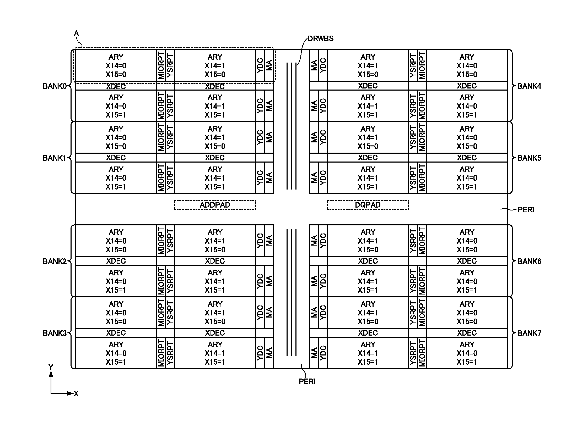
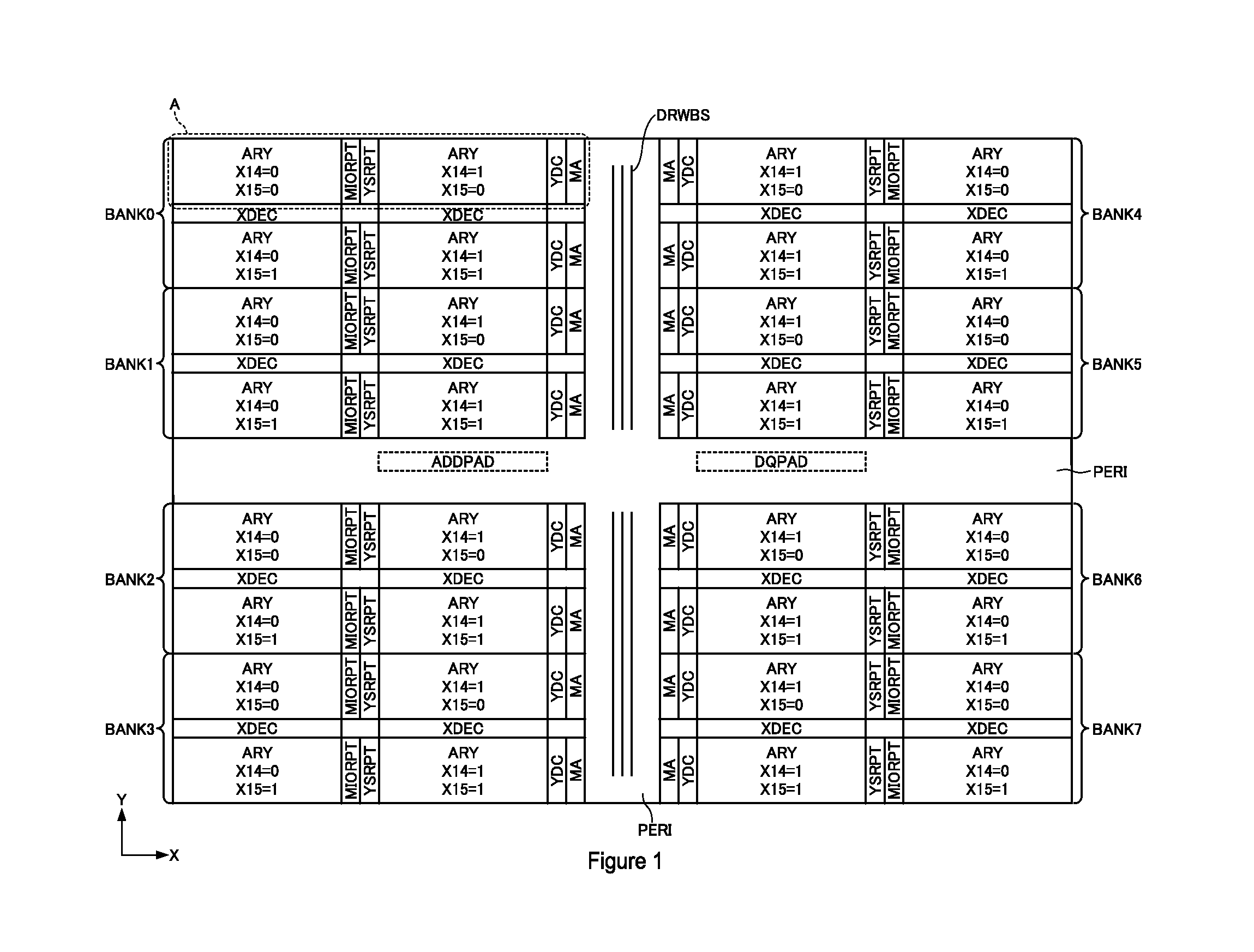
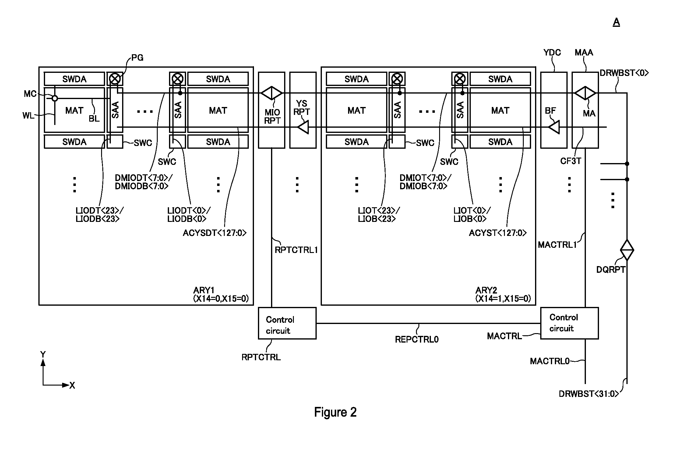
[0056]FIG. 1 is a schematic plan view showing the entire layout of a semiconductor device according to an embodiment of the present invention.

[0057]As shown in FIG. 1, a semiconductor device according to this embodiment includes a plurality of memory cell arrays ARY arranged in matrix and a peripheral circuit area PERI provided between the memory cell arrays ARY. In this embodiment, four memory cell arrays ARY constitute one memory bank. A memory bank herein refers to a unit that is mutually non-exclusively accessible. As shown in FIG. 1, in this embodiment, memory banks BANK0 to BANK3 are arranged on one side of a chip in the X-direction (left side), and memory banks BANK4 to BANK7 are arranged on the other side in the X-direction (right side).

[0058]In addition, at the center of the chip in the Y-direction, a peripheral circuit area PERI extending in the X-direction is provided, and external terminals, such as an address terminal ADDPAD and a data terminal DQPAD, are arranged in th...


PUM


Abstract

A semiconductor memory disclosed in this disclosure includes first and second memory cell arrays, a first main data line that transfers the read data read from the first memory cell array, a second main data line that transfers the read data read from the second memory cell array, a main amplifier coupled to the second main data line, and a repeater circuit coupled to the first main data line and the second main data line.

Description

[0001]This application is based upon and claims the benefit of priority from Japanese Patent Application No. 2013-221945 filed on Oct. 25, 2013, the disclosure of which are incorporated herein in its entirely by reference.BACKGROUND[0002]Field of Invention[0003]The present invention relates to a semiconductor device. It particularly relates to a semiconductor device including a main data line that transfers data read from a memory cell array to a main amplifier.[0004]Description of the Related Art[0005]In semiconductor devices, such as DRAM (Dynamic Random Access Memory), the reduction of chip size is important for the reduction of chip unit price. The reduction of chip size in DRAM can be achieved mainly by reducing the size of a memory cell array, and the size reduction percentage in peripheral circuits tends to be lower as compared with the memory cell array. Accordingly, the proportion of peripheral circuits in the entire chip has been increasing year by year, and, in order to f...

Claims


Application Information

Patent Timeline
Patent Type & Authority Patents(United States)
IPC IPC(8): G11C7/00G11C11/4096G11C11/4094G11C11/4091G11C7/12G11C7/10G11C7/08G11C5/02
CPCG11C5/025G11C7/08G11C7/1048G11C7/1051G11C7/1069G11C7/12G11C11/4091G11C11/4094G11C11/4096
Inventor MITSUBORI, SHINGOFUJISAWA, HIROKI
Owner MICRON TECH INC
Why Eureka
Try Eureka