Front electrode with thin metal film layer and high work-function buffer layer for use in photovoltaic device and method of making same

a technology of photovoltaic devices and buffer layers, which is applied in the direction of basic electric elements, electrical apparatus, and semiconductor devices, can solve the problems of insufficient conductivity, difficult to make front electrodes made solely of zinc oxide tco layers, and tend to suffer from darkening, so as to reduce the potential barrier for holes extracted, and be made more cheap and/or fast

Inactive Publication Date: 2008-05-08
GUARDIAN GLASS LLC
View PDF99 Cites 76 Cited by
  • Summary
  • Abstract
  • Description
  • Claims
  • Application Information

AI Technical Summary

Benefits of technology

[0003]Typical TCOs used for certain front electrodes of photovoltaic devices are n-type and therefore can create a Schottky barrier at the interface between the TCO and the uppermost semiconductor layer of the photovoltaic device (e.g., p-type silicon based layer) in a reverse direction to the built-in field. This barrier can act as a barrier for holes extracted from the device by the front electrode, thereby leading to inefficient performance.
[0004]Thus, it will be appreciated that there exists a need in the art for an improved front electrode for a photovoltaic device which can reduce the potential barrier for holes extracted from the photovoltaic device by the front electrode.
[0005]In order to overcome the aforesaid problem, the front electrode of the photovoltaic device is provided with both: (a) a transparent metal (or substantially metallic) film of a material such as Cu, Ag, Au, Ni, Pd, Al, alloys thereof, a combination of one or more of these metals with other metal(s), or the like, and (b) a transparent high work-function buffer layer. The transparent metal film may be a low work-function film in certain example embodiments. The high-work function buffer layer is located between the metal film and the uppermost semiconductor layer of the photovoltaic device so as t...

Problems solved by technology

In many instances, the transparent front electrode is formed of a single layer using a method of chemical pyrolysis where precursors are sprayed onto the glass substrate at approximately 400 to 600 degrees C. Front electrodes made solely of an F-doped tin oxide TCO layer are undesirable in that they tend to suffer from darkening in hydrogen atmo...

Method used


Image

  • Front electrode with thin metal film layer and high work-function buffer layer for use in photovoltaic device and method of making same
  • Front electrode with thin metal film layer and high work-function buffer layer for use in photovoltaic device and method of making same
  • Front electrode with thin metal film layer and high work-function buffer layer for use in photovoltaic device and method of making same

Examples


Embodiment Construction

[0014]Referring now more particularly to the drawings in which like reference numerals indicate like parts throughout the several views.

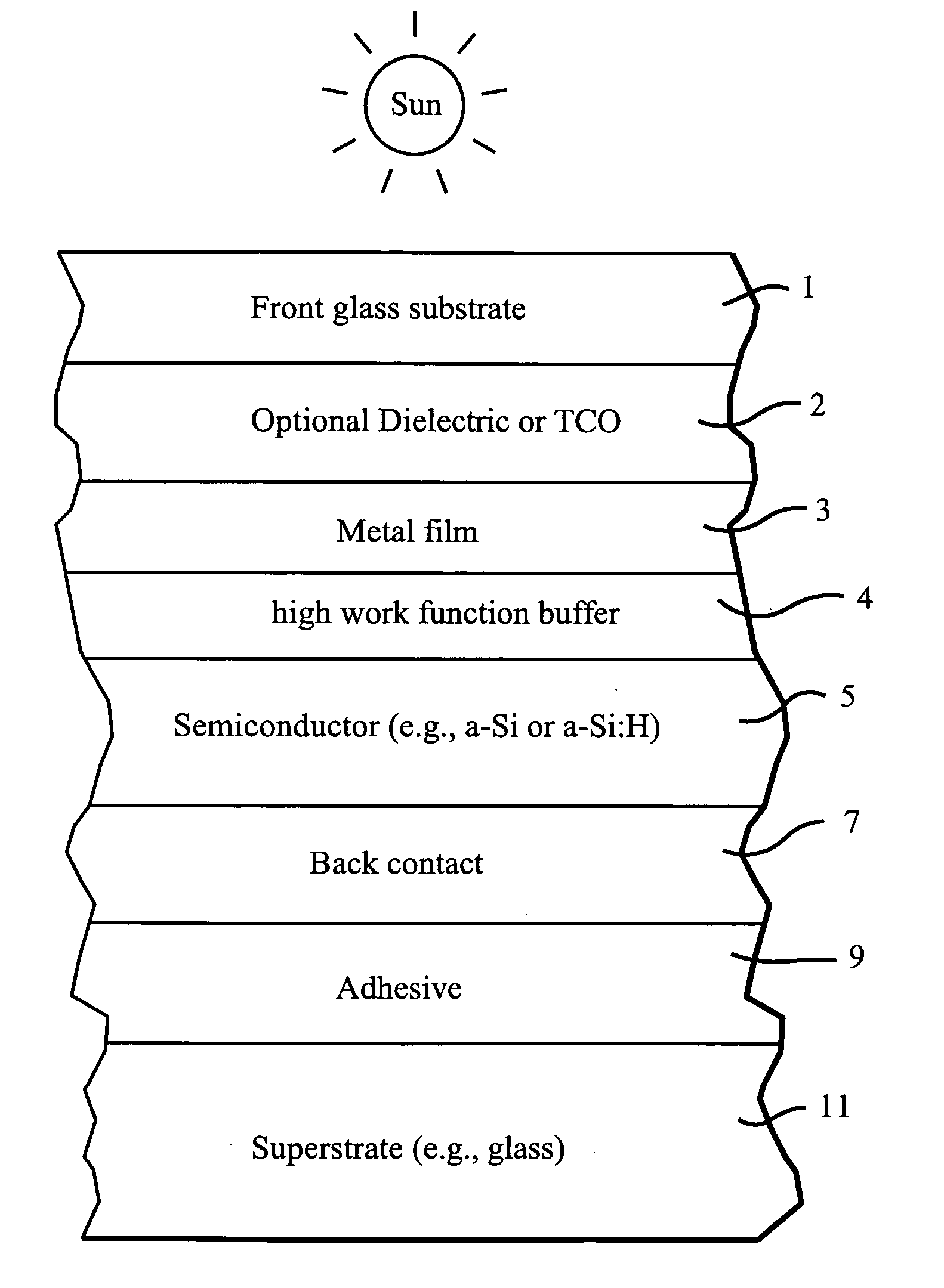
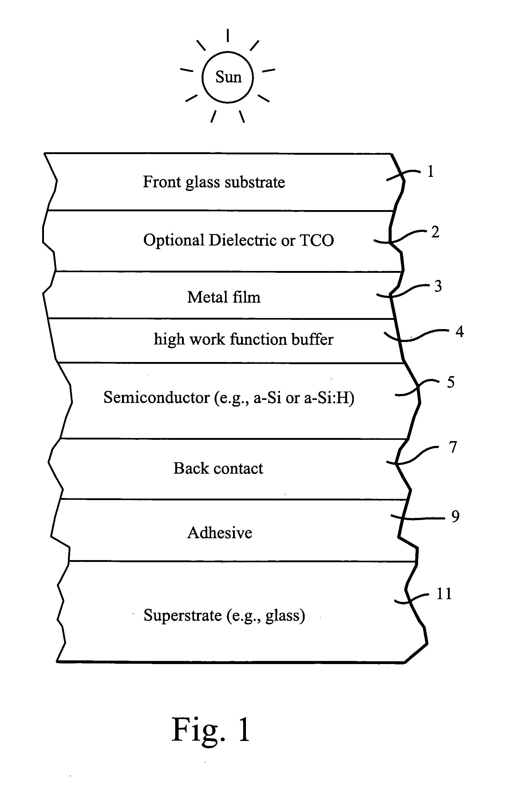
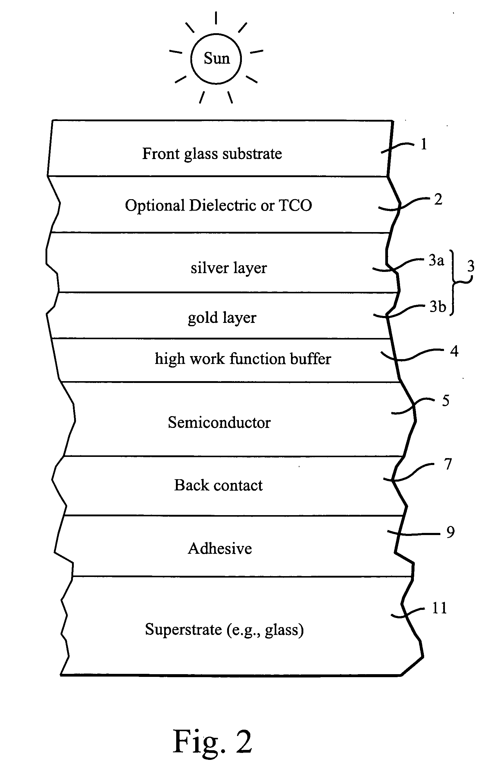
[0015]Photovoltaic devices such as solar cells convert solar radiation and other light into usable electrical energy. The energy conversion occurs typically as the result of the photovoltaic effect. Solar radiation (e.g., sunlight) impinging on a photovoltaic device and absorbed by an active region of semiconductor material (e.g., a semiconductor film including one or more semiconductor layers such as a-Si layers) generates electron-hole pairs in the active region. The electrons and holes may be separated by an electric field of a junction in the photovoltaic device. The separation of the electrons and holes by the junction results in the generation of an electric current and voltage. In certain example embodiments, the electrons flow toward the region of the semiconductor material having n-type conductivity, and holes flow toward the region of the ...


PUM


Abstract

This invention relates to a front electrode or contact for use in an electronic device such as a photovoltaic device. In certain example embodiments, the front electrode of the photovoltaic device includes a highly conductive metal film and a thin high work-function buffer layer. The high-work function buffer layer is located between the metal film and the uppermost semiconductor layer so as to provide for substantial work-function matching between the metal film and the high work-function uppermost semiconductor layer so as to reduce a potential barrier for holes extracted from the device by the front electrode/contact. Optionally, a layer such as a transparent conductive oxide (TCO) or a dielectric may be provided between a front glass substrate and the metal film.

Description

[0001]This invention relates to a photovoltaic device including a front electrode / contact. In certain example embodiments, the front electrode of the photovoltaic device includes a highly conductive metal film and a thin high work-function buffer layer. The high-work function buffer layer is located between the metal film and the uppermost semiconductor layer of the photovoltaic device so as to provide for substantial work-function matching between the metal film and the high work-function uppermost semiconductor layer of the device in order to reduce a potential barrier for holes extracted from the device by the front electrode / contact. Optionally, a layer such as a transparent conductive oxide (TCO) or a dielectric may be provided between a front glass substrate and the metal film in certain example instances.BACKGROUND AND SUMMARY OF EXAMPLE EMBODIMENTS OF INVENTION[0002]Photovoltaic devices are known in the art (e.g., see U.S. Pat. Nos. 6,784,361, 6,288,325, 6,613,603, and 6,123...

Claims


Application Information

Patent Timeline
IPC IPC(8): H01L31/0224H01L31/04
CPCH01L31/022425Y02E10/50H01L31/022466
Inventor KRASNOV, ALEXEY
Owner GUARDIAN GLASS LLC
Why Eureka
Try Eureka