
On chip test mode implementation

Inactive Publication Date: 2008-05-08
RPX CORP
View PDF11 Cites 14 Cited by
  • Summary
  • Abstract
  • Description
  • Claims
  • Application Information

AI Technical Summary

Benefits of technology

[0015]One objective of the present invention is to provide a method that reduces the time required for a PTC test on an image sensor device and thereby lowers production cost.
[0016]A further objective of the present invention is to provide a method that reduces the time needed for a dark current test while checking for image sensor pixel defects.
[0017]A still further objective of the present invention is to improve the accuracy of the PTC and dark current tests by implementing an exposure matrix in a “snap shot mode”.

Problems solved by technology

However, process variations during CMOS image sensor fabrication and other factors such as particle defects on the surface of the image sensor cause the output of certain pixels to vary either above or below the desired output range.
If a large enough number of the pixels in the array fail to provide an acceptable output signal, the image sensor is rejected.
Testing is a major cost component of the final image sensor device because of the large number of pixels that must be tested, and the nature of the test which includes both optical and electrical methods.
The parasitic leakage may be significant for long read out times (long exposures).
Since common light sources are not programmable and fast switching, it is generally not feasible to vary the illumination (photon flux) during the frame.
Moreover, changing the intensity of the light source from one exposure to the next is less accurate than changing the exposure level by varying the time for a fixed illumination.
Changing the light intensity will result in intensity differences from one frame to the next of about 1% or less but that variability is enough to produce less accurate calculations than when intensity is kept constant and exposure time is varied.
As a result, improvements in PTC and dark current test throughput are limited because of the multiple number of frames required in the standard test method.
However, the method does not address the lengthy acquisition times necessary for pixel illumination and dark current tests.

Method used


Image

  • On chip test mode implementation
  • On chip test mode implementation
  • On chip test mode implementation

Examples


Embodiment Construction

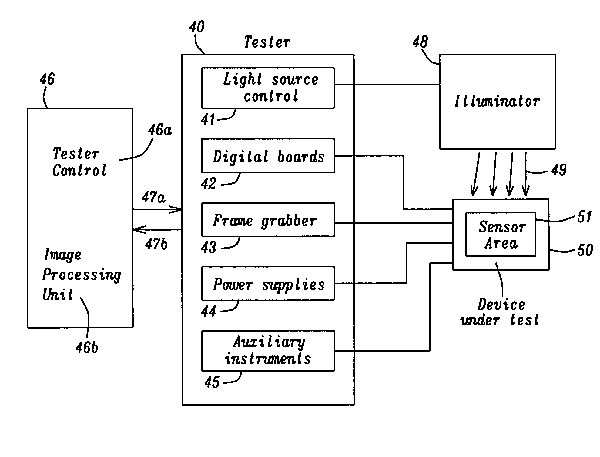
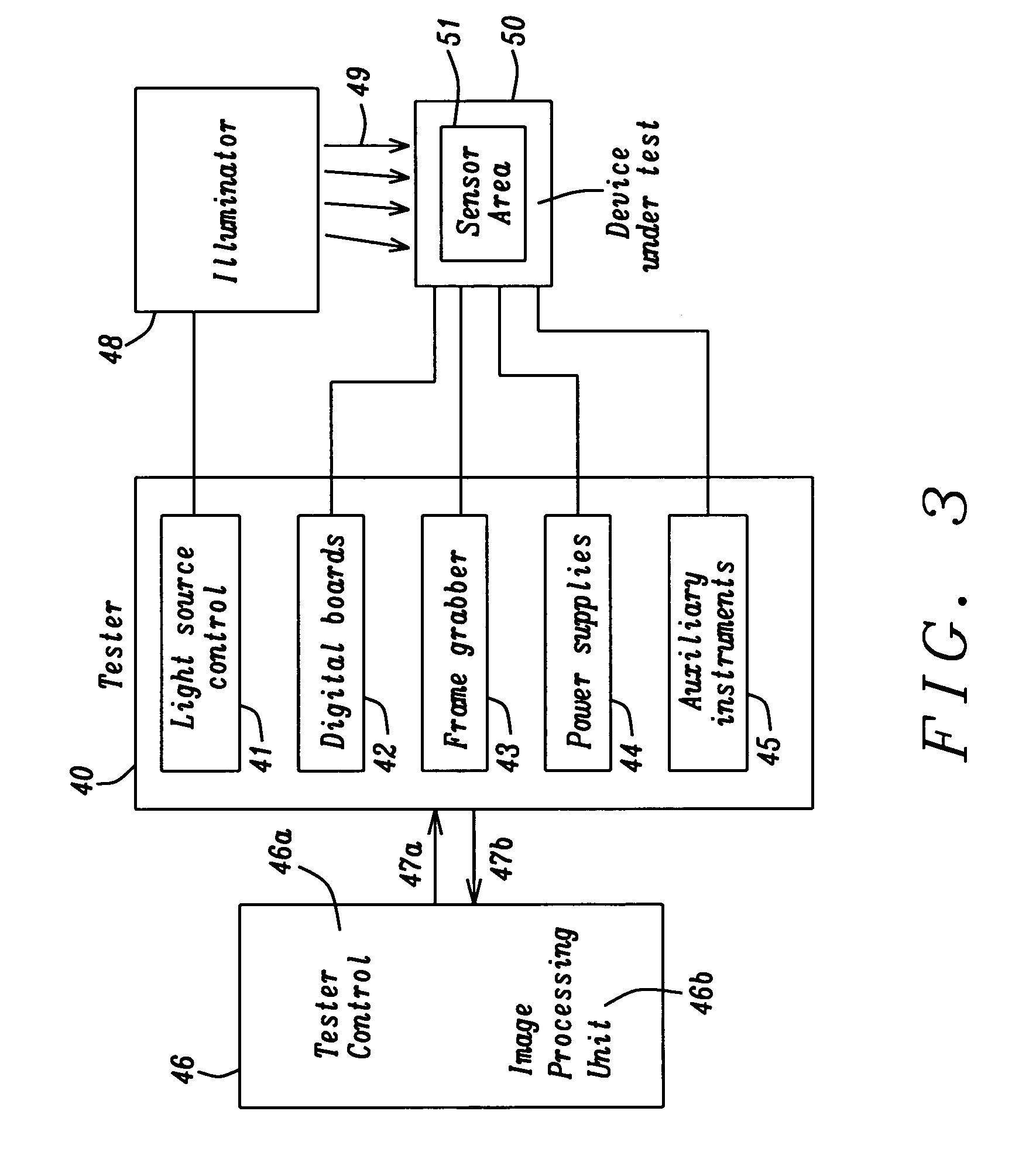
[0027]The present invention is a method of improving the throughput of the photon transfer curve (PTC) test and dark current test when checking the reliability of pixels in an image sensor device. The drawings are provided by way of example and are not intended to limit the scope of the invention. The terms “exposure” and “illumination” may be used interchangeably.

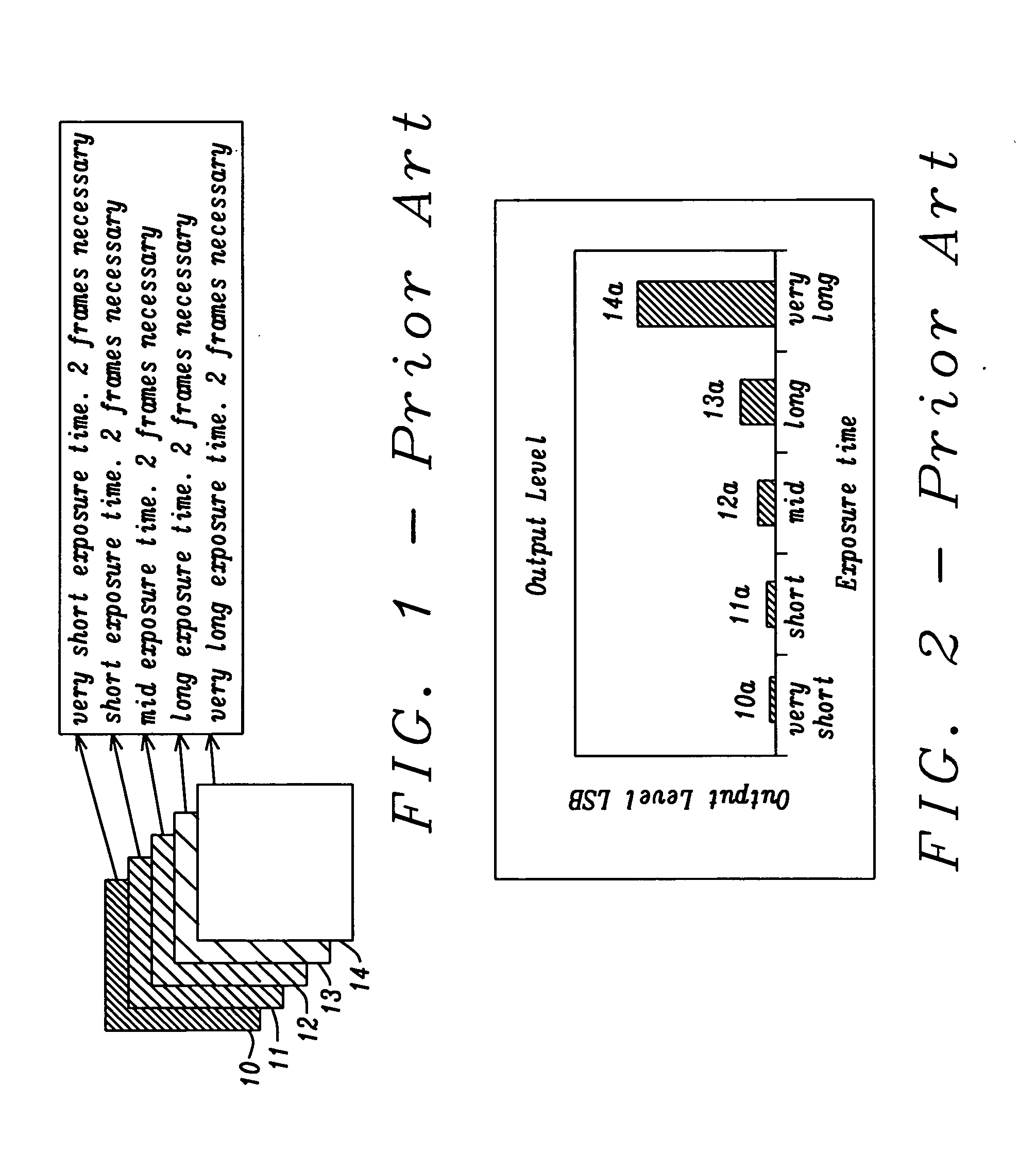
[0028]The inventors have previously practiced a PTC and dark current test method wherein between five and ten different illumination levels involving two frames each are used to provide PTC measurements, and an additional set of frames (5 to 10) without illumination are needed for dark current calculations. For example, in FIG. 1, images 10-14 resulting from five different exposure times (illumination levels) during a PTC test are illustrated. In other words, the illumination portion of the PTC test has been divided into steps such that each pair of two frames is uniformly illuminated for a certain time. The illumination t...


PUM


Abstract

An improved on chip test method for determining the photon transfer curve (PTC) and dark current in an image sensor is described. Cost and time savings is achieved by reducing the number of frames necessary for the measurements to three including two exposure frames and one frame for dark current testing. A conventional test involving “n” different exposure times each with two frames is replaced by implementing a snap shot mode where a first plurality of pixel rows are exposed for a time t1, a second plurality of pixel rows are exposed for a time t2, and so forth up to an nth plurality of pixel rows exposed for a time tn where the total number of pixel rows equals a frame and tn>t2>t1. The resulting image has “n” regions each with a different brightness that become progressively brighter from top to bottom of the image.

Description

RELATED PATENT APPLICATION[0001]This application is related to the following: Docket # DS05-002, Ser. No. ______, filing date ______, assigned to a common assignee.FIELD OF THE INVENTION[0002]The invention relates to an improved method of testing pixels in a CMOS image sensor. In particular, the time required for photon transfer curve (PTC) testing and dark current testing is reduced and test accuracy is increased by implementing an exposure matrix in a snap shot mode.BACKGROUND OF THE INVENTION[0003]A complementary metal oxide semiconductor (CMOS) image sensor is a key component of many digital video cameras and other “high tech” devices. The CMOS image sensor is typically comprised of an upper stack that includes one or more layers of color filters and a microlens array, and a lower stack that includes interlevel dielectric layers, interlevel metal layers, and passivation layers that are formed on a substrate. The function of the microlens component is to focus incident light thro...

Claims


Application Information

Patent Timeline
IPC IPC(8): H04N17/00H04N5/353
CPCH04N17/002H04N5/3535H04N25/533
Inventor NUSSBACHER, MARK
Owner RPX CORP
Learn More