

IC package keeping attachment level of leads on chip during molding process
- Summary
- Abstract
- Description
- Claims
- Application Information
AI Technical Summary
Benefits of technology
Problems solved by technology
Method used
Image

Examples
first embodiment
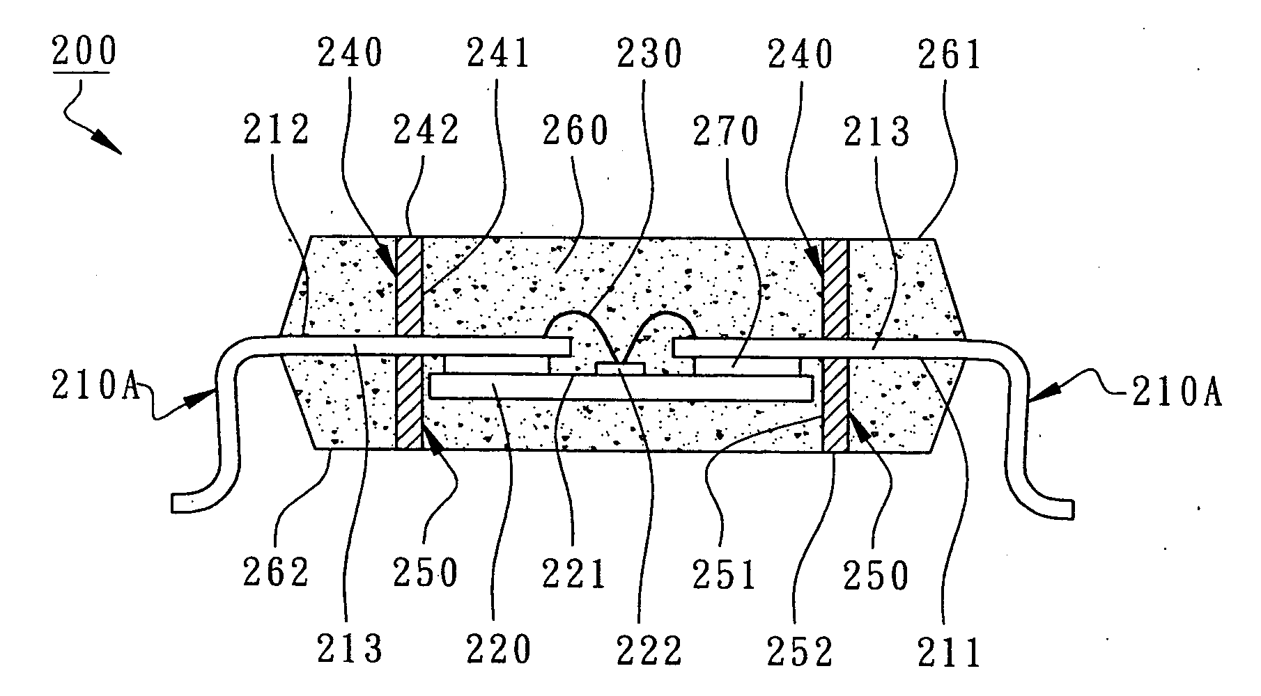
[0018]In the present invention, FIG. 2 shows a cross-sectional view of an IC package keeping attachment level of leads on chip during molding process. FIG. 3 shows a plan view of the semiconductor package prior to encapsulation.
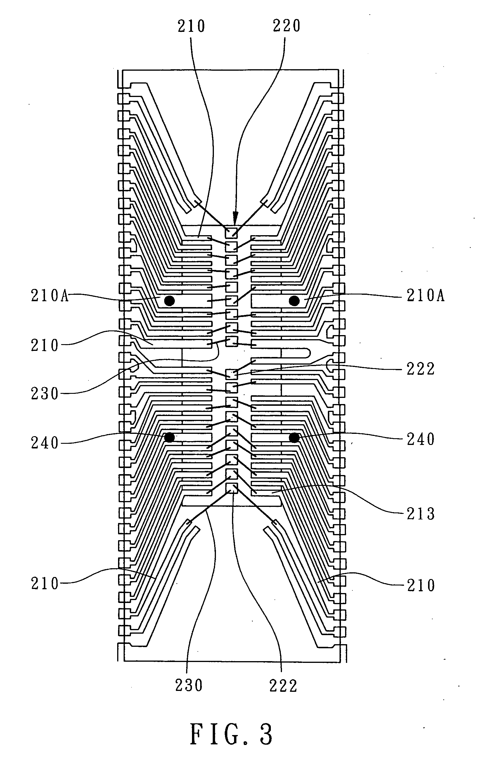
[0019]Referring to FIGS. 2 and 3, a semiconductor package 200 mainly comprises a plurality of leads of a LOC leadframe including 210, 210A, a chip 220, a plurality of bonding wires 230, a plurality of first supporting columns 240, a plurality of second supporting columns 250 and a molding compound 260. Referring now to FIG. 3, the leads not connected with the first supporting columns 240 are marked with reference number “210” and the leads connected to the first supporting columns 240 are marked with reference number “210A”. Referring to FIGS. 2 and 3, the LOC leadframe has no die pad, a plurality of chip-attaching tapes 270 or other chip-attaching materials are applied to adhere an active surface 221 of the chip 220 to the lower surfaces 211 of the leads 210...
second embodiment
[0026]In the present invention, another IC package keeping attachment level of leads on chip during molding process is disclosed. Referring to FIG. 4, a semiconductor package 300 mainly comprises a plurality of leads 310 of a LOC leadframe, a chip 320, a plurality of bonding wires 330, a molding compound 340 and a plurality of supporting columns 350. The active surface 321 of the chip 320 is attached to the lower surfaces 311 of the leads 310 with a plurality of chip-attaching tapes 360. The chip 320 has a plurality of bonding pads 322 located at a center area of the active surface 321 and electrically connected to the leads 310 by the bonding wires 330. The molding compound 340 encapsulates the chip 320, the bonding wires 330 and inner portions 313 of the leads 310. The supporting columns 350 are optionally disposed on the lower surfaces 311 or upper surfaces 312 of some of the leads 310 where displacement occurs frequently and adjacent the chip 320 to keep attachment level of chip...
PUM
 Abstract
Description
Claims
Application Information