Printed circuit board and fabricating method thereof

a printed circuit board and printed circuit technology, applied in the direction of printed circuit non-printed electric components association, printed element electric connection formation, conductive pattern formation, etc., can solve the problem that conventional multi-layer pcb is limited to be applied to slim products, and achieve the effect of thin thickness

Inactive Publication Date: 2008-05-22
SAMSUNG ELECTRONICS CO LTD
View PDF3 Cites 26 Cited by
  • Summary
  • Abstract
  • Description
  • Claims
  • Application Information

AI Technical Summary

Benefits of technology

[0014]Accordingly, the present invention has been made to solve the above-mentioned problems occurring in the prior art and provides additional advantages, by providing a PCB capable of achieving a multi-layer structure with a thinner thickness.

Problems solved by technology

Further, since two or more cores are attached to each other, there is a problem in that the conventional multi-layer PCB is limited to be applied to slim products.

Method used


Image

  • Printed circuit board and fabricating method thereof
  • Printed circuit board and fabricating method thereof
  • Printed circuit board and fabricating method thereof

Examples


Embodiment Construction

[0026]Hereinafter, exemplary embodiments of the present invention will be described with reference to the accompanying drawings. For the purposes of clarity and simplicity, a detailed description of known functions and configurations incorporated herein will be omitted as it may make the subject matter of the present invention unclear.

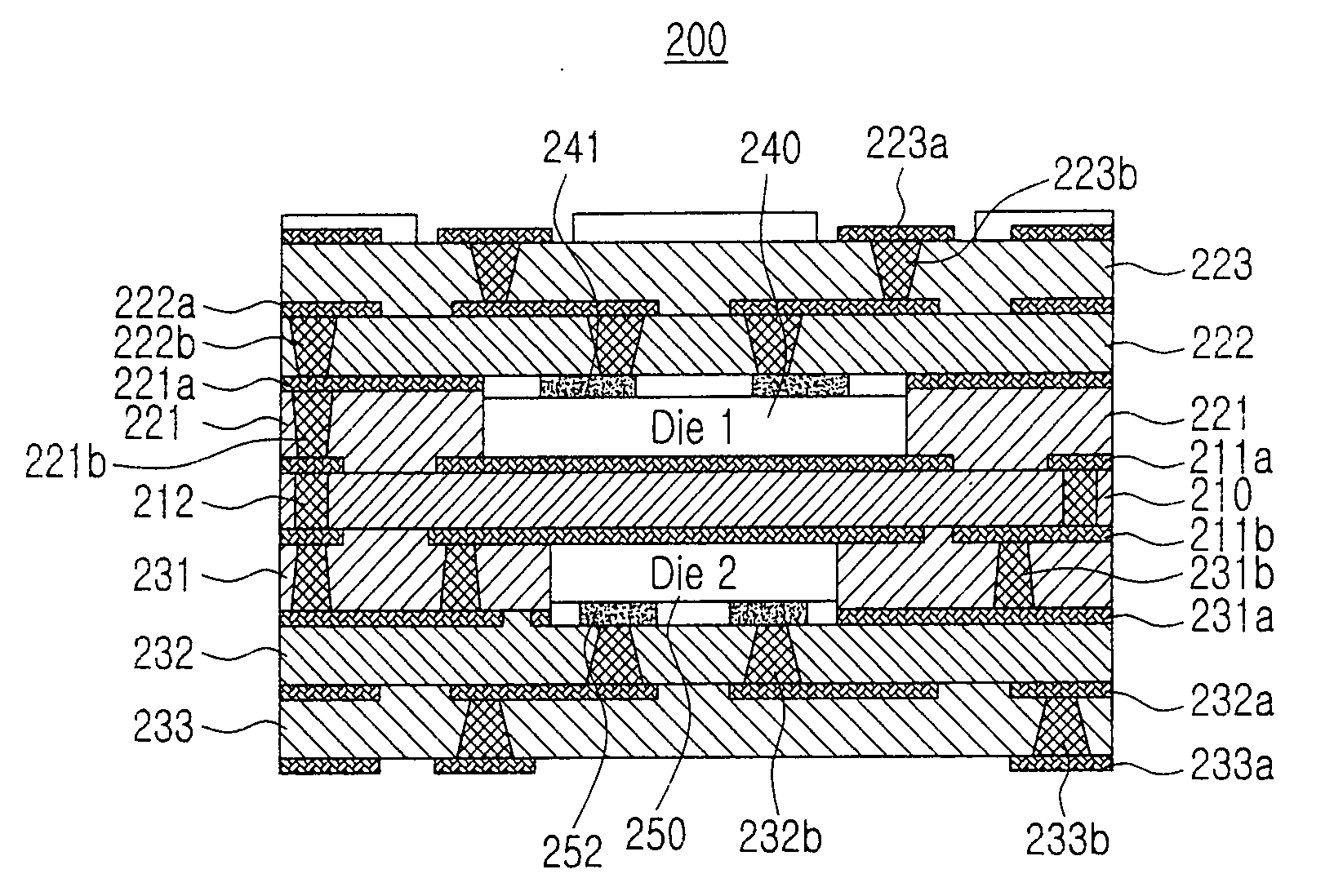
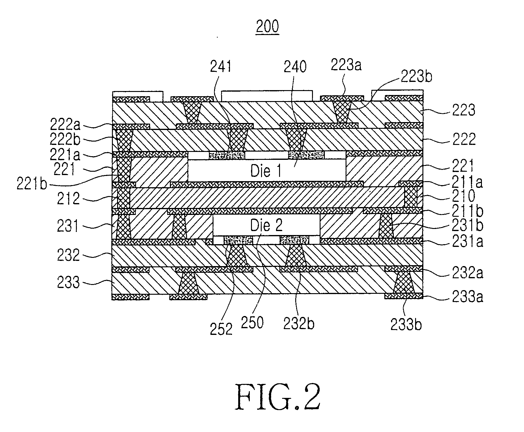
[0027]FIG. 2 is a sectional view of a multi-layer PCB in accordance with an exemplary embodiment of the present invention. As shown, the multi-layer PCB 200 of the present invention includes a core 210, a plurality of insulation layers 221-223 and 231-133 and a plurality of conductive pattern layers 211a, 211b, 221a, 222a, 223a, 231a, 232a, and 233a alternatively formed on each of both sides of the core 210, a plurality of via holes 212, 221b, 222b, 223b, 231b, 232b and 233b formed through the core 210 and the insulation layers 221-223 and 231-133, and first and second semiconductor dies 240 and 250.

[0028]The via holes 212, 221b, 222b, 223b, 231b, 232b...


PUM

PropertyMeasurementUnit
conductiveaaaaaaaaaa
adhesive strengthaaaaaaaaaa
densityaaaaaaaaaa

Abstract

Disclosed are a multi-layer PCB and a fabricating method thereof. The multi-layer PCB includes: a core; a plurality of insulation layers and a plurality of conductive pattern layers alternatively stacked on both sides of the core; and a plurality of via holes formed through the core and the insulation layers. The fabricating method may includes the steps of: forming a conductive pattern layer on each of both sides of a core, and forming via holes through the core; attaching a double-stick tape with weak adhesive strength to a portion of each of a upper surface and a lower surface of the core; and forming an insulation layer on each of a upper surface and a lower surface of the core to cover the double-stick tapes, and forming a conductive pattern layer on each of the insulation layers.

Description

CLAIM OF PRIORITY[0001]This application claims the benefit under 35 U.S.C. §119(a) of an application entitled “Printed Circuit Board And Fabricating Method Thereof,” filed in the Korean Intellectual Property Office on Nov. 22, 2006 and assigned Serial No. 2006-115676, the contents of which are hereby incorporated by reference.BACKGROUND OF THE INVENTION[0002]1. Field of the Invention[0003]The present invention relates to a multi-layer printed circuit board (multi-layer PCB), and more particularly to a multi-layer PCB which has semiconductor dies (or integrated circuits) embedded (or seated) thereinside.[0004]2. Description of the Related Art[0005]PCBs are used in various types of electric products. Especially, the multi-layer PCB, which has a layered structure including insulation layers and conductive pattern layers stacked alternatively, is used in electronic devices requiring high-density integration, such as a notebook computer, a portable radiotelephone, etc.[0006]FIG. 1A is a ...

Claims


Application Information

Patent Timeline
Patent Type & Authority Applications(United States)
IPC IPC(8): H05K1/18H05K1/02H05K3/10H05K3/42
CPCH01L24/18Y10T29/49165H01L25/0657H01L2224/18H01L2224/82039H01L2225/06524H01L2924/01075H01L2924/14H05K1/185H05K3/0035H05K3/4614H05K3/4652H05K2201/09127H01L2924/01006H01L2924/01033H01L24/82H01L24/19H01L2224/04105H01L2224/73267H01L2224/92244H01L2924/15153H05K1/11
Inventor SEO, HO-SEONGLEE, YOUNG-MINCHO, SHI-YUNCHOI, YOUN-HOKIM, SANG-HYUN
Owner SAMSUNG ELECTRONICS CO LTD
Why Eureka
Try Eureka