Porous and dense hybrid interconnect structure and method of manufacture

a hybrid interconnect and dense technology, applied in the field of porous and dense hybrid interconnect structures, can solve the problems of significant challenge, low k dielectric materials with relatively weak mechanical properties compared to dense dielectric materials, and conventional chemical mechanical process (cmp) has difficulty polishing a low mechanical-module porous dielectric. achieve the effect of high performan

Inactive Publication Date: 2008-05-29
IBM CORP
View PDF11 Cites 14 Cited by
  • Summary
  • Abstract
  • Description
  • Claims
  • Application Information

AI Technical Summary

Problems solved by technology

Capacitance improvements can be made with porous low k dielectrics; however, porous low k dielectric materials have relatively weak mechanical properties as compared to dense dielectrics.
It is also a significant challenge for the current BEOL process to integrate these porous low k dielectrics with other module processes.
For example, the conventional chemical mechanical process (CMP) has difficulty polishing a low mechanical-module porous dielectric.
However, by making the entire dense dielectric material porous, the structure presents weak mechanical properties inside the final interconnect structure.

Method used


Image

  • Porous and dense hybrid interconnect structure and method of manufacture
  • Porous and dense hybrid interconnect structure and method of manufacture
  • Porous and dense hybrid interconnect structure and method of manufacture

Examples


Embodiment Construction

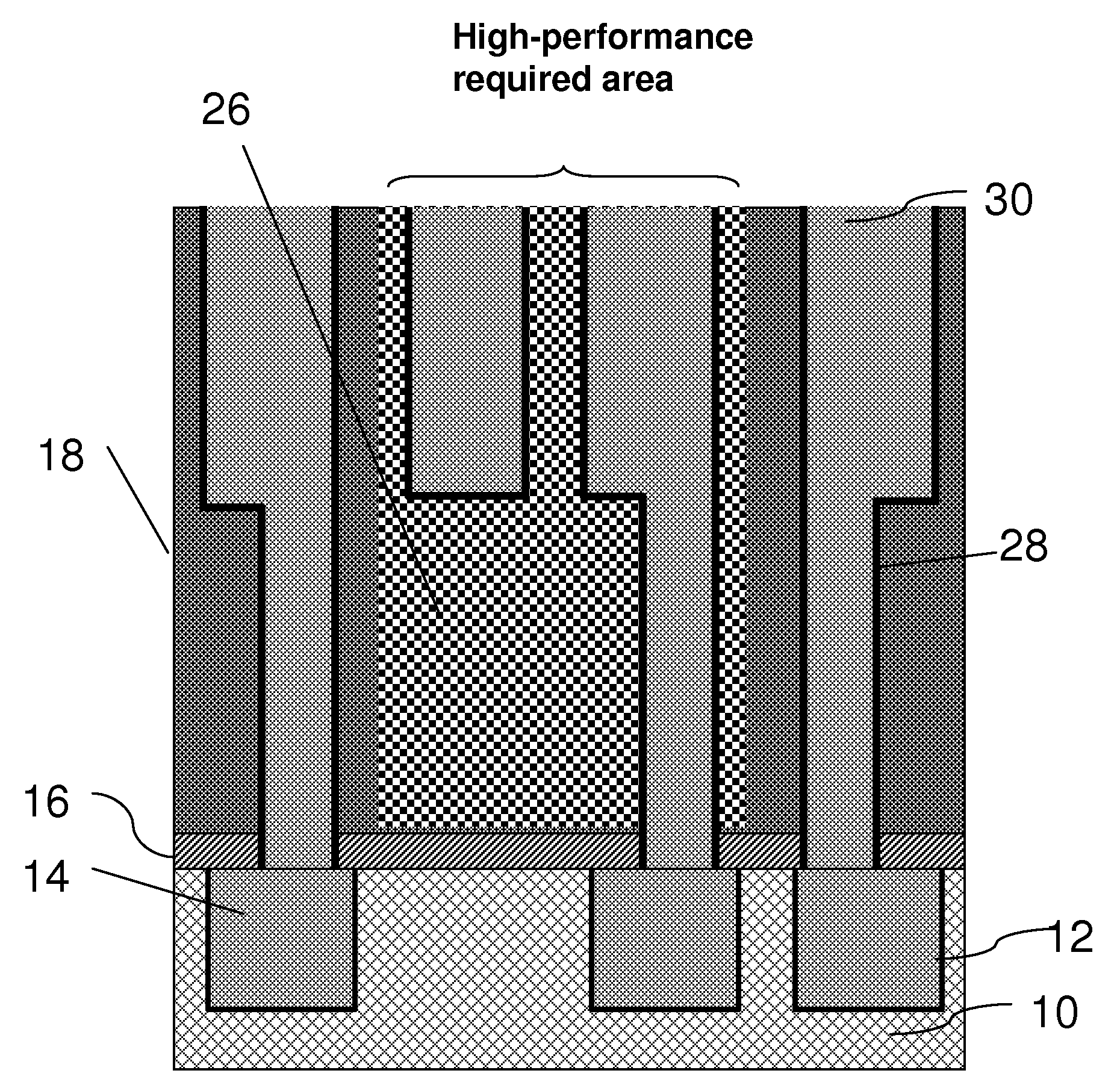
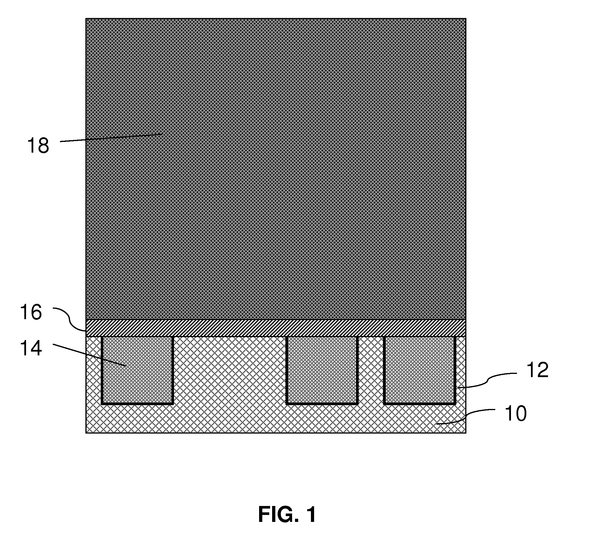
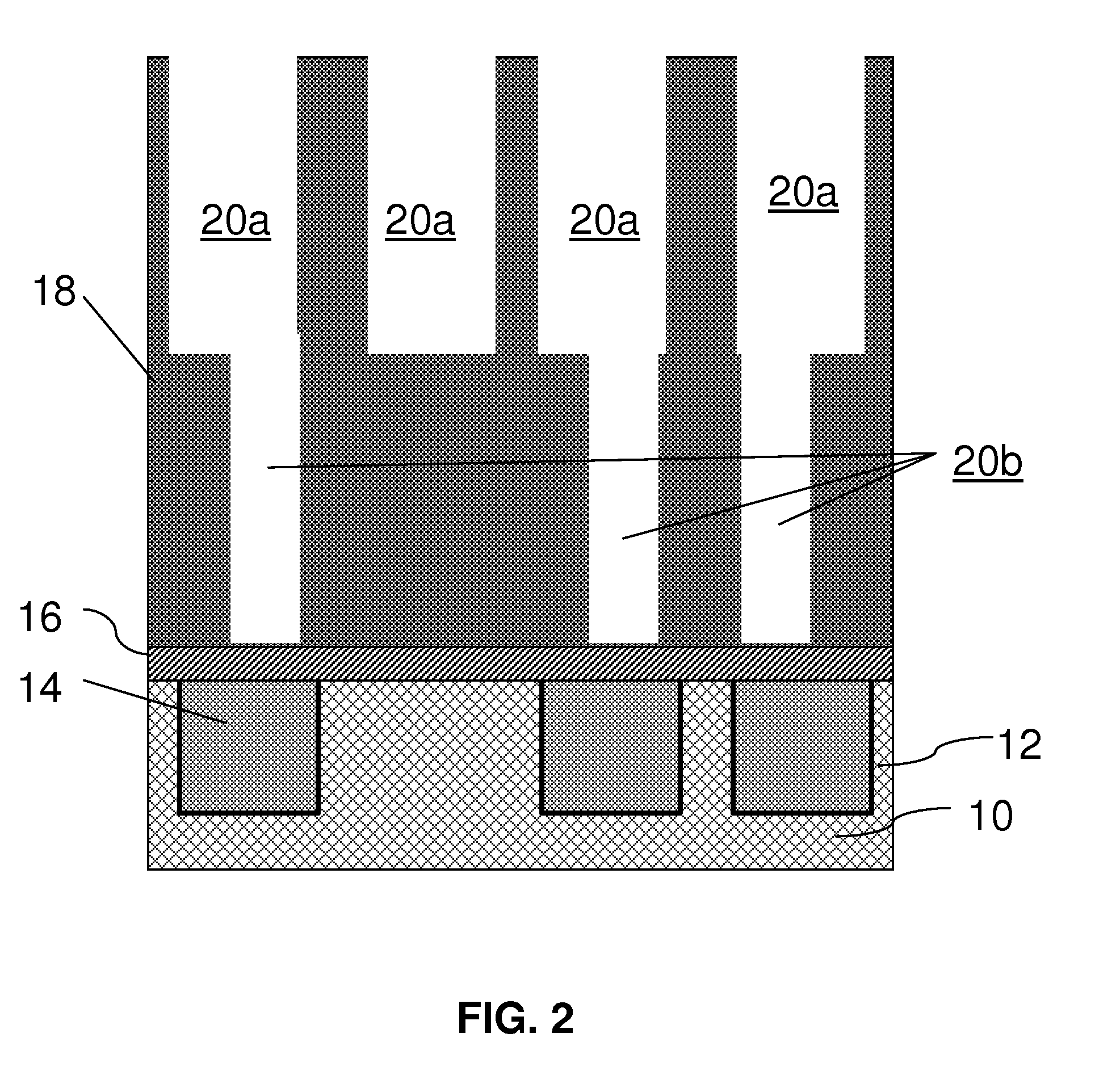
[0014]The invention is directed to semiconductor structures and methods for manufacturing, and more particularly to porous and dense hybrid interconnect structures for high performance and reliability semiconductor applications and methods of manufacturing such structure. In embodiments, the structure fabricated using the processes described herein is a hybrid interconnect structure with porous dielectric for high performance required areas and dense dielectric for high reliability required areas. More specifically, in embodiments of the invention, porous dielectric is formed at areas that require low dielectric capacitance for electrical performance improvement, while dense dielectric is used at areas that required high mechanical strength for overall reliability enhancement of the structure. As such, in embodiments, the interconnect structure of the invention contains both dense and porous “hybrid” dielectrics inside a dielectric material for overall BEOL capacitance reduction and...


PUM

PropertyMeasurementUnit
temperatureaaaaaaaaaa
dielectric capacitanceaaaaaaaaaa

Abstract

A method for manufacturing a structure includes depositing a dense dielectric over the entire wafer, which includes areas that require low dielectric capacitance and areas that require high mechanical strength. The method further includes masking areas of the dense dielectric over the areas that require high mechanical strength and curing unmasked areas of the dense dielectric to burn out porogens inside the dense dielectric and transform the unmasked areas of the dense dielectric to porous dielectric material. A semiconductor structure comprises porous and dense hybrid interconnects for high performance and reliability semiconductor applications.

Description

FIELD OF THE INVENTION[0001]The invention generally relates to semiconductor structures and methods of manufacturing such structures, and more particularly to porous and dense hybrid interconnect structures for high performance and reliability semiconductor applications and methods of manufacturing such structures.BACKGROUND DESCRIPTION[0002]In order to reduce the back end of line (BEOL) interconnect portion of a circuit delay, a conventional silicon dioxide dielectric (k of approximately 4.0) has been replaced with dense lower-k films with a k value of approximately 3.0. However, for further performance improvements, more dielectric capacitance reduction is required (k<2.5) for advanced devices.[0003]Capacitance improvements can be made with porous low k dielectrics; however, porous low k dielectric materials have relatively weak mechanical properties as compared to dense dielectrics. It is also a significant challenge for the current BEOL process to integrate these porous low k...

Claims


Application Information

Patent Timeline
Patent Type & Authority Applications(United States)
IPC IPC(8): H01L23/522H01L21/768
CPCH01L21/7682H01L21/76835H01L23/53295H01L23/53238H01L23/5329H01L23/5222H01L2924/0002H01L2221/1047H01L2924/00
Inventor YANG, CHIH-CHAOWONG, KEITH KWONG HONYANG, HAINING
Owner IBM CORP
Why Eureka
Try Eureka