Fault detection method, test circuit and semiconductor device

a fault detection and fault technology, applied in the direction of coding, pulse technique, instruments, etc., can solve the problems of inability to accurately circuit failure to carry out the correct operation, and error detection so as to and accurately and positively detect the fault of the delay chain

Inactive Publication Date: 2008-05-29
SOCIONEXT INC
View PDF4 Cites 5 Cited by
  • Summary
  • Abstract
  • Description
  • Claims
  • Application Information

AI Technical Summary

Benefits of technology

[0007]Another and more specific object of the present invention is to provide a fault detection method, a test circuit and a semiconductor device, which can accurately and positively detect a fault in a delay chain, even if the pulse width of the signal input to or output from the delay chain is extremely narrow or the signal frequency input to or output from the delay chain is extremely high.
[0008]Still another object of the present invention is to provide a fault detection method for detecting, within a semiconductor device, a fault in a delay chain that is provided within the semiconductor device and is made up of a plurality of delay parts that are each formed by a plurality of delay cells, comprising a first judging step judging whether or not a fault of a first specific delay cell within a first delay part exists when testing the first specific delay cell, by detecting a first relative delay time between input and output signals of the first specific delay cell, and processing the first relative delay time at a timing based on an output of a delay cell within a second delay part that is provided at a stage preceding or subsequent to the first delay part; and a second judging step judging whether or not a fault of a second specific delay cell within the second delay part exists when testing the second specific delay cell, by detecting a second relative delay time between input and output signals of the second specific delay cell, and processing the second relative delay time at a timing based on an output of a delay cell within the first delay part. According to the test circuit of the present invention, it is possible to accurately and positively detect a fault in a delay chain, even if the pulse width of the signal input to or output from the delay chain is extremely narrow or the signal frequency input to or output from the delay chain is extremely high.
[0009]A further object of the present invention is to provide a test circuit for a delay chain made up of a plurality of delay parts that are each formed by a plurality of delay cells, comprising a first test circuit configured to test a first specific delay cell within a first delay part by detecting a first relative delay time between input and output signals of the first specific delay cell; and a second test circuit configured to test a second specific delay cell within a second delay part that is provided at a stage preceding or subsequent to the first delay part by detecting a second relative delay-time between input and output signals of the second specific delay cell, wherein the first test circuit judges whether or not a fault of the first specific delay cell exists by processing the first relative delay time at a timing based on an output of a delay cell within the second delay part, and the second test circuit judges whether or not a fault of the second specific delay cell exists by processing the second relative delay time at a timing based on an output of a delay cell within the first delay part. According to the test circuit of the present invention, it is possible to accurately and positively detect a fault in a delay chain, even if the pulse width of the signal input to or output from the delay chain is extremely narrow or the signal frequency input to or output from the delay chain is extremely high.
[0010]Another object of the present invention is to provide a semiconductor device comprising a delay chain, provided on a substrate, and made up of a plurality of delay parts that are each formed by a plurality of delay cells; and a test circuit provided on the substrate, the test circuit comprising a first test circuit configured to test a first specific delay cell within a first delay part by detecting a first relative delay time between input and output signals of the first specific delay cell; and a second test circuit configured to test a second specific delay cell within a second delay part that is provided at a stage preceding or subsequent to the first delay part by detecting a second relative delay time between input and output signals of the second specific delay cell, wherein the first test circuit judges whether or not a fault of the first specific delay cell exists by processing the first relative delay time at a timing based on an output of a delay cell within the second delay part, and the second test circuit judges whether or not a fault of the second specific delay cell exists by processing the second relative delay time at a timing based on an output of a delay cell within the first delay part. According to the semiconductor device of the present invention, it is possible to accurately and positively detect a fault in a delay chain, even if the pulse width of the signal input to or output from the delay chain is extremely narrow or the signal frequency input to or output from the delay chain is extremely high.

Problems solved by technology

In such a semiconductor circuit, if a certain delay cell fails, the delay chain cannot generate the correct delay, and the circuit cannot carry out the correct operation.
Accordingly, there was a problem in that it is impossible to accurately detect the fault of the delay chain when the pulse width of the signal input to or output from the delay chain is extremely narrow or the signal frequency input to or output from the delay chain is extremely high.

Method used


Image

  • Fault detection method, test circuit and semiconductor device
  • Fault detection method, test circuit and semiconductor device
  • Fault detection method, test circuit and semiconductor device

Examples


Embodiment Construction

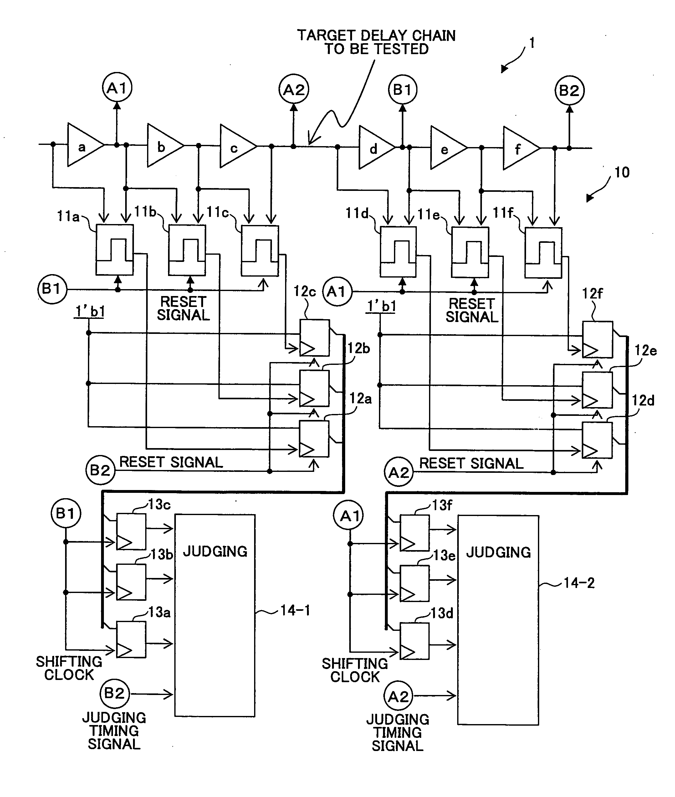
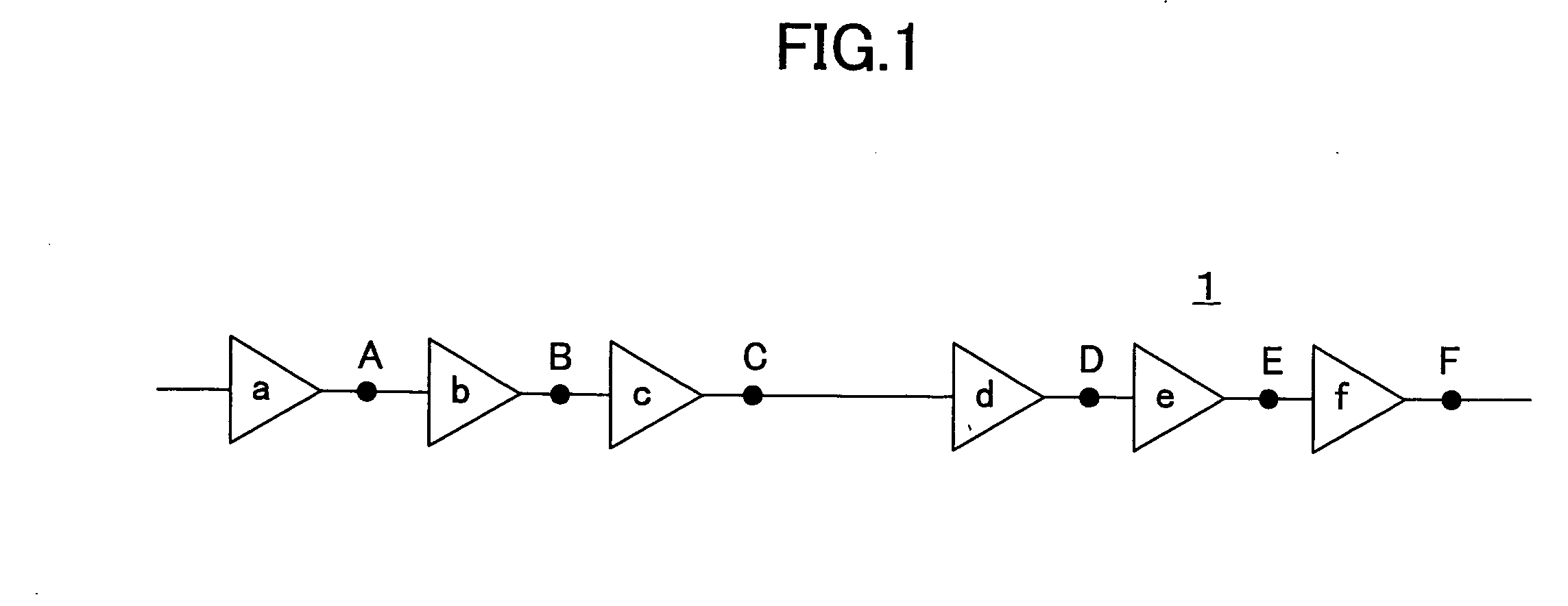
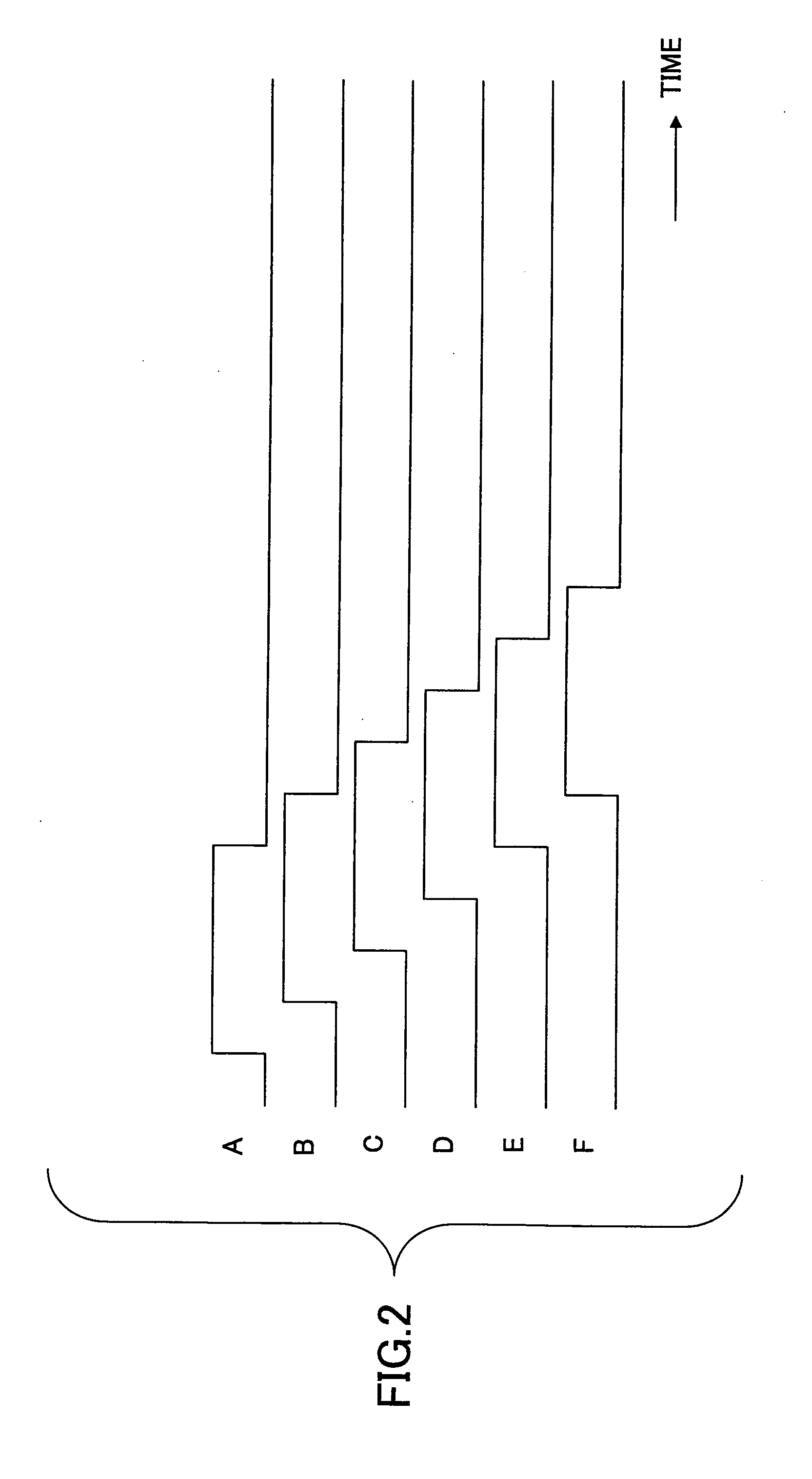
[0029]A fault detection method of the present invention detects a fault in a delay chain of a semiconductor circuit within a semiconductor device, using a test circuit within the semiconductor device. The delay chain is made up of a plurality of delay parts that are connected in series, where each delay part has a plurality of delay cells. In a case where the delay chain is formed by two delay parts and a specific delay cell within a first delay part is to be tested, a relative delay time between input and output signals of this specific delay cell is detected, and the relative delay time is processed at a timing that is based on an output of a specific delay cell within a second delay part that is connected to a stage subsequent to the first delay part, so as to judge whether or not a fault exists in the specific delay cell within the first delay part. When testing the specific delay cell within the second delay part, a relative delay time between input and output signals of this s...


PUM


Abstract

A fault detection method for detects, within a semiconductor device, a fault in a delay chain that is provided within the semiconductor device and is made up of delay parts that are each formed by delay cells. The method judges if a fault exists in a first specific delay cell within a first delay part when testing the first specific delay cell, by detecting a first relative delay time between input and output signals of the first specific delay cell, and processing the first relative delay time at a timing based on an output of a delay cell within a second delay part that is provided at a stage preceding or subsequent to the first delay part. The method judges if a fault exists in a second specific delay cell within the second delay part exists when testing the second specific delay cell, by detecting a second relative delay time between input and output signals of the second specific delay cell, and processing the second relative delay time at a timing based on an output of a delay cell within the first delay part.

Description

BACKGROUND OF THE INVENTION[0001]1. Field of the Invention[0002]The present invention generally relates to fault detection methods, test circuits and semiconductor devices, and more particularly to a fault detection method for detecting a fault in a circuit that has a delay chain, a test circuit using such a fault detection method, and a semiconductor device having such a test circuit.[0003]2. Description of the Related Art[0004]Semiconductor devices having a delay chain made up of a plurality of delay cells are known. One example of the semiconductor circuit having the delay chain is a delay locked loop (DLL) circuit which controls and adjusts a time difference between an external clock and an internal clock by circuitry, so as to realize a high-speed clock access (or short clock access time) and a high operation frequency. In such a semiconductor circuit, if a certain delay cell fails, the delay chain cannot generate the correct delay, and the circuit cannot carry out the correct ...

Claims


Application Information

Patent Timeline
Patent Type & Authority Applications(United States)
IPC IPC(8): G01R31/28H01L21/822H01L27/04H03K5/14
CPCG01R31/3016H03K5/133G01R31/31703
Inventor YAMANAKA, HIROAKI
Owner SOCIONEXT INC
Why Eureka
Try Eureka