Semiconductor memory device having improved voltage transmission path and driving method thereof

Active Publication Date: 2008-05-29
SAMSUNG ELECTRONICS CO LTD
View PDF11 Cites 23 Cited by
  • Summary
  • Abstract
  • Description
  • Claims
  • Application Information

AI Technical Summary

Benefits of technology

[0013]Embodiments of the present invention provide a semiconductor memory device and a driving method thereof which are capable of providing a stable voltage signal to a memory cell of the semiconductor memory device.

Problems solved by technology

However, in this configuration, a feed / sink path of the voltage signals becomes relatively long, which hampers performance characteristics of the chip 10.
As a result, the performance of the entire memory system deteriorates.

Method used


Image

  • Semiconductor memory device having improved voltage transmission path and driving method thereof
  • Semiconductor memory device having improved voltage transmission path and driving method thereof
  • Semiconductor memory device having improved voltage transmission path and driving method thereof

Examples


Embodiment Construction

[0024]The present invention will now be described more fully hereinafter with reference to the accompanying drawings, in which exemplary embodiments of the invention are shown. This invention may, however, be embodied in many different forms and should not be construed as being limited to the embodiments set forth herein. Rather, these embodiments are provided so that this disclosure will be thorough and complete, and will fully convey the scope of the invention to those skilled in the art. In the drawings, the thickness of layers and regions are exaggerated for clarity. Like numbers refer to like elements throughout the specification.

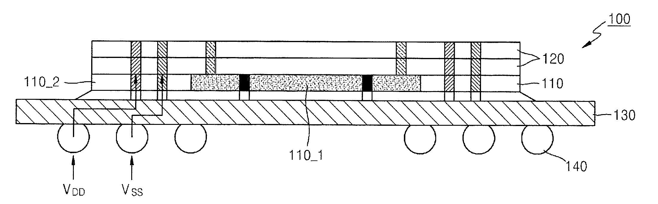
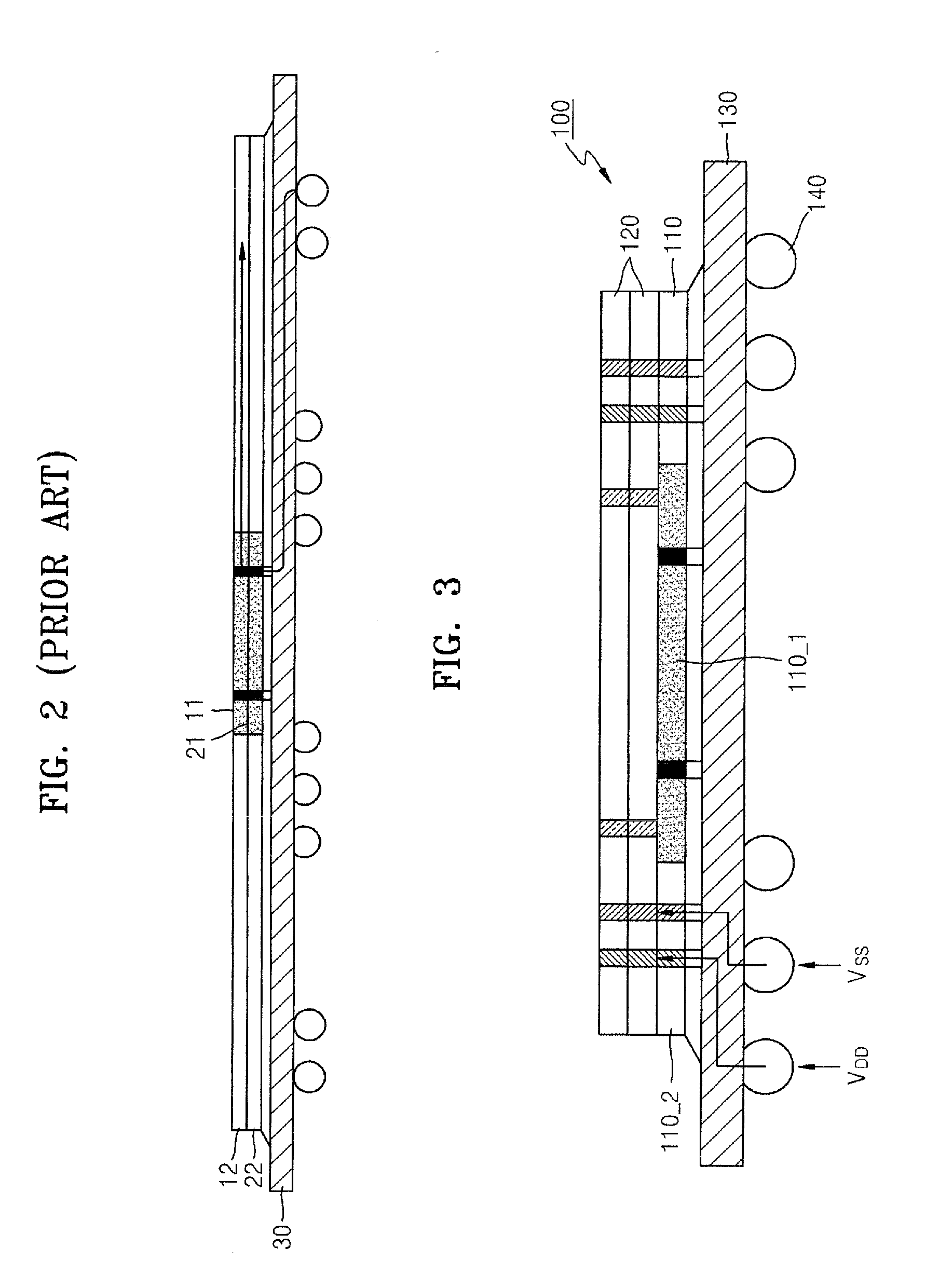
[0025]FIG. 3 is a cross-sectional view of a semiconductor memory device 100 according to an embodiment of the present invention. The semiconductor memory device 100 shown in a packaged form may include a first semiconductor chip 110 that includes an input / output circuit for sending / receiving a voltage signal, a data signal and a control signal, etc. to...


PUM


Abstract

Provided are a semiconductor memory device and a method of driving the device which can improve a noise characteristic of a voltage signal supplied to a memory cell of the device. The semiconductor memory device includes a first semiconductor chip and one or more second semiconductor chips stacked on the first chip. The first chip includes an input / output circuit for sending / receiving a voltage signal, a data signal, and a control signal to / from an outside system. The one or more second semiconductor chips each include a memory cell region for storing data. The second semiconductor chips receive at least one signal through one or more signal paths that are formed outside the input / output circuit of the first chip.

Description

CROSS-REFERENCE TO RELATED PATENT APPLICATION[0001]This application claims the benefit of Korean Patent Application No. 10-2006-0117087, filed on Nov. 24, 2006, in the Korean Intellectual Property Office, the disclosure of which is incorporated herein by reference.BACKGROUND[0002]1. Field of the Invention[0003]The present invention relates to a semiconductor memory device and a driving method thereof, and more particularly, to a semiconductor memory device and a driving method thereof that are capable of improving a noise characteristic of a voltage signal provided to a memory cell of the semiconductor memory device.[0004]2. Description of the Related Art[0005]In recent years, the capacity and speed of memory chips, which are used as memory devices in electronic systems, have increased. Furthermore, various attempts to increase memory capacity per unit area and to drive the memory more rapidly have been made.[0006]FIG. 1 is a schematic view of a general conventional semiconductor ch...

Claims


Application Information

Patent Timeline
IPC IPC(8): G11C5/06
CPCG11C5/063H01L25/0657H01L25/18H01L2225/06541H01L2225/06513H01L2225/06517H01L2224/16145H01L2224/05573H01L2224/13025H01L2924/00014H01L2224/0554H01L2224/05599H01L2224/0555H01L2224/0556G11C7/10G11C5/14
Inventor KANG, SUN-WONBAEK, SEUNG-DUK
Owner SAMSUNG ELECTRONICS CO LTD
Why Eureka
Try Eureka